8645A Agile Signal Generator: when disaster strikes

For a long time I have been looking for a reasonably prices 8645A, and finally, I found one – with the note “doesn’t power up”. Well, most likely, a defective power supply. The 8645A and some related generators (not the 8643A) use linear supplies, because these are really low noise devices, and a switching supply just doesn’t seem to do the trick. Interesting, because for the very quiet 8662A/8663A signal generators, HP was relaying on switches supplies…. maybe they just could not fit anything else.

Back to the 8645A – this is no less than a miracle, a marvelous apparatus. No idea how many manhours (man-decades) of engineering went into it. It’s complexity, and subtle detail, nothing short of a moon landing vehicle, made for an electronic test lab. They way HP designed the shielding, and implemented a rigorous low leakage approach, this alone is worth special admiration.

Even better, the unit discussed here has option 1, which is an OCXO high stability reference, and it has a build-in doubler, extending the frequency range to above 2 GHz. About USD $50k in 1990, nowadays, nobody can afford such build quality anymore.

Well, all these are good reasons for looking forward to soon doing some repairs on such kind of unit, and make it “power up again”. Well, that was the thought.

This issue: while many hours of hard work went into fabricating this thing, not more than a few seconds were spent, to consider adequate packaging, to ship a box, 80 pounds.

8645a damage

8645a damage 2

8645a damage 3

8643a damage 4

Such kind of damage, not seen before. Except for the little bit of Instapak, no other protecting foam or anything – nothing to hold it in place in the box. The result – a badly damaged front panel, broken input connector, and even the front frame, damaged beyond repair.
Just the single front end connector (which has an internal airline, gold plated) – USD 200+; the machine, it seems beyond repair.

The only good news – the seller (who did not package it himself) seems to be a very resonable person, so we will work something out. To be continued.

Micro-Tel MSR-904A Microwave Receiver: reducing phase noise – phase detector frequency

Like with most PLL build, there a quite a few things that can go wrong – the result: a lot of phase noise. For the current setup, all precautions had been taken to avoid bad surprises – low noise supplies, well-proven loop filter amplifier, low noise DAC, adequate cables. And, phase lock was quickly achieved (see last post).
For more detailed analysis, both the 160 MHz and the 21.4 MHz IF signals of the MSR-904A are fed to analyzers. For the 160 MHz, to a RTL SDR stick, just for the rough picture, and the 21.4 MHz, to a 3585A analyzer. The 3585A has very low noise, ideally suited to look at phase noise, except if you are working the ultra low noise segment.

Initial finding – phase noise is down at about 60 dBc at >10 kHz offset, dropping off as expected, but the close-in noise is really bad. Close in noise often related to the phase detector, or the reference. Substituting the 10 MHz reference from the EIP545A by a really low noise HP 10 MHz OCXO didn’t change much. So to high noise level must be connected to phase detector.

With the detector set to 1.25 MHz (:8 reference divider), there we can gain quite a few dB of noise supression, by increasing the detector frequency (within limits, doubling the detector frequency lowers the associated noise contribution by about 3 dB). And, even more, we can check out the reference doubler, which is a build-in feature of the ADF4157. With the doubler in use, it needs to be ensured that the duty cycle of the reference is close to 50%, but this is ensured by the OCXO anyway.

The ADF4157 can handle phase detector frequencies of up to 32 MHz, no issue at all with 20 MHz. The only downside – more fractional-N spurs – channel spacing for integer only dividers is now 160 MHz, rather than 10 MHz….

msr pll phase noise

msr pll phase noise averaged

Red and green traces – you can see, the PLL is completely detector noise saturated within the bandwidth.

Other traces – all with a phase detector frequency of 20 MHz – and at different charge pump currents (CPC). A CPC of 15 corresponds to a 5 mA current. This has direct impact on the phase loop cut-off frequency. There is some peaking, at 2 kHz (dark blue trace, CPC 1), and at about 7 kHz, light blue trace, CPC 10.

Comparing the yellow and magenta traces – these differ by the 10 MHz reference signal source only (yellow uses an HP 10811 OXCO, magenta uses the EIP 545A build-in reference which is pretty stable, but rather noisy). In the curent setup, both references yield very similar results – accordingly, the noise within the PLL bandwidth is dominated by the PLL cirucit itself, and the phase detector, not the reference source.

There are some mains-related spurs at 60 and 180 Hz, but these might just be due to the temporary cabling and lack of a proper case. The circuit is fully exposed, tranformers closeby, etc. For the final setup, all cables will need to be as short as possible, especially for the pretune voltage (which is about 2 MHz per Volt – 2 kHz noise for 1 mV!).

Credits go to KE5FX for the great PN.EXE phase noise measurement tool, invaluable for any such work!

Micro-Tel MSR-904A Microwave Receiver: phase lock test, YIG driver bandwidth modification

Some final parts added to the MSR-904A digital interface/PLL: the actual PLL circuit (frontend), an Analog Devices ADF4157 fractional-N PLL, together with an ADF5002 8:1 prescaler. The phase detector is set at 1.25 MHz, to allow 10 MHz integer-only steps. Some experimentation with other phase detector frequencies might follow later.

Here – the schematic of the PLL frontend. The circit is wired point-to-point, sure enough, with VERY short wires, soldered using a microscoped – hope you have a steady hand. After a quick test (using the MUX output of the ADF4157), the wires and the very tiny ADF gadgets, all sealed with a few drops of epoxy.

msr pll adf5002 adf4157 schematic

On the main board, the PLL loop filter. Build around the remaining half of the already installed OPA2703 (other half used for the DAC output buffer).

msr pll loop filter

With all these parts now put together, to do some basic tests on the PLL – a Gigatronics 605 Microwave Synthesizer was connected to the MSR-904A input, and the LO sample output of the MSR-904A connected to PLL. A sample of the “LO sample” taken by a broadband -10 dB coupler is used to monitor the frequency, using an EIP 545A. The 10 MHz reference output of the EIP is used as the ADF4157 reference.

msr pll phase lock test setup
msr pll test setup 2

The MSR-904A down-converts the signal to a first 250 MHz IF (by fundamental LO), the 250 MHz IF is then mixed with 410 MHz (this can be locked to a 5 MHz signal – not locked at the moment, but the signal is very clean and stable anyway).

The 160 MHz 2nd IF is available at the rear panel, and connected to a R820T RTL SDR. This is a very handy method to monitor noise, and do some basic adjustments on the PLL. Using headphones – and the human ear as a phase noise meter… more quantitative analysis to follow.

Here, the transition from manually controlled CW mode, to PLL controlled mode.
msr-904a locked at 7250 mhz lo

A close-up:
msr-904a locked at 7250 mhz lo 2

For these tests, the LO was locked at 7.25 GHz, receiving a signal at 7.0 GHz (SDR offset set to about 160 MHz).

Note – same as for the Micro-Tel 1295, and the SG-811 – the YIG driver has a bandwidth limit (by a 100 uF Tantalum capacitor – and a 499 k resistor!) that is controlled by a reed relais on the YIG driver. This doesn’t allow low phase noise operation, even with the best PLL. Well, 100 uF is a bit too much. Therefore, a 100 n capacitor was added – this is enough to suppress most of the noise of the YIG driver stage, and still the circuit remains fast enough for full band sweeps at moderate scan rates. Might modify this later, by adding a bit of logic that adds the 100 n capacitor only when the external frequency control is active, but disconnects it during full band sweep, etc.
msr-904a YIG driver board

Micro-Tel MSR-904A Interface/PLL: low noise power supplies for PLL and pretune circuits

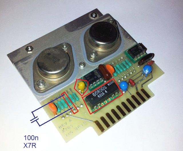
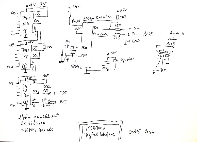
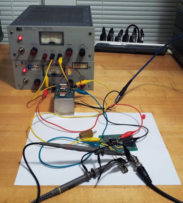
Recently, some pretune DAC and microcontroller circuitry has been build, see earlier post. This is now basically functional, however, we need to confirm that is is really working as desired. Never trust any circuits just build – especially when it comes to “unpredictable” aspects like noise. The parts used, they will most likely perform up to their specification, but there can be all kinds of hidden issues that will later on lead to lengthy troubleshooting of phase noise or spur issues.
From experience, power supply related noise is one of the most severe and troublesome item, if not taken care of at an early stage of design, or prototype construction.

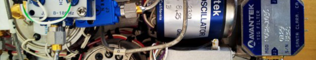
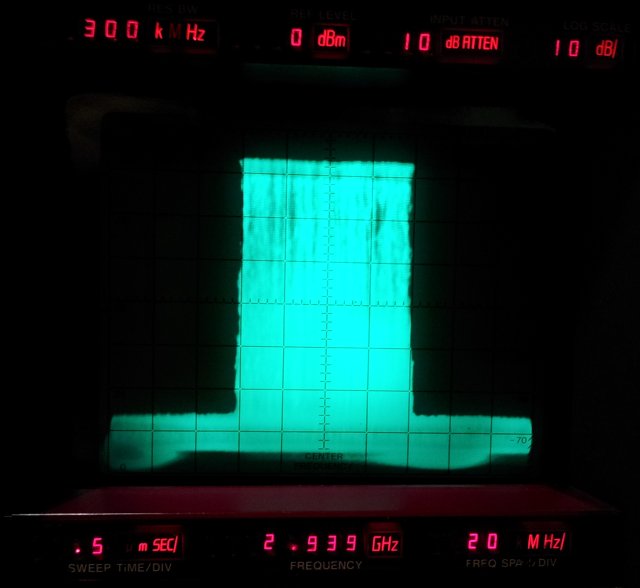
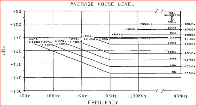
Many articles exist on how to characterize power supply noise, especially at very low levels. This is not really what we need here, because we are talking about a real-world circuit that will later work with a mains power supply, in a reasonably well shielded case. So, our standard will be the lowest noise analyzer I have around here, an HPAK (HP Agilent, now: Keysight) 3585A Spectrum analyzer. This has pretty low noise anyway, down to -137 dBm for a 3 Hz bandwidth.

msr pll 3585a noise floor

The only downside of the 3585A, it is about 80 pounds – you will need a sturdy bench and a strong assistant to lift it.
msr pll 3585a analyzer
As a side note: The instrument on my bench, it has an interesting sticker, formerly owned by ST (STMicroelectronics, formerly known as SGS-Thomson as printed on the cal label). ST does a pretty massive amount of R&D in the field of semiconductors, and has a long-standing history of inventions. Well, fair enough, I got this instrument in bad shape, seems to have passed through many hands since ST time, but it is now fully repaired and calibrated, providing great service.

Step (1) – analysis of the circuits already build. Just some 0-25 kHz spectra.

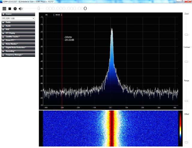
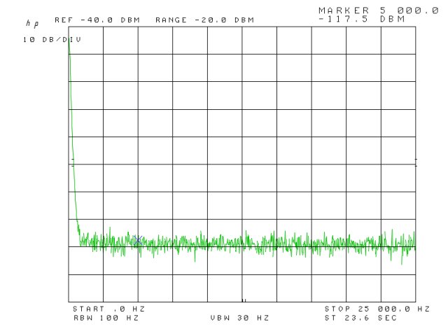
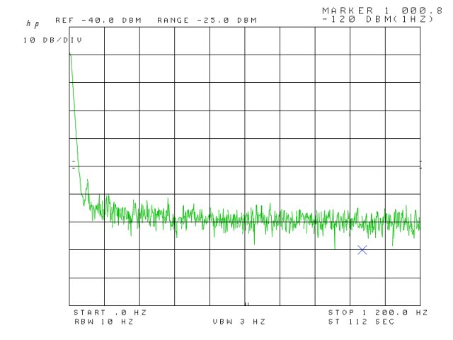
Noise floor, probe grounded at AGND.
msr pll agnd floor 25k

317 regulator output (11.4 V)
msr pll 317 noise 25k

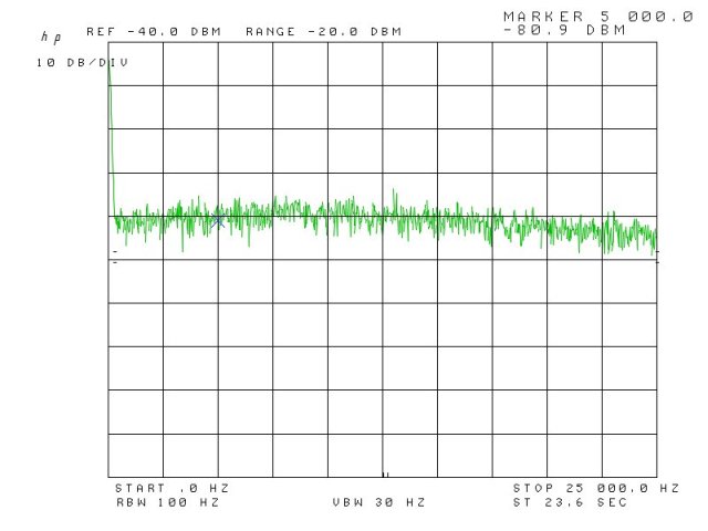
– well, much worse than expected! More than 30 dB above the noise level!!

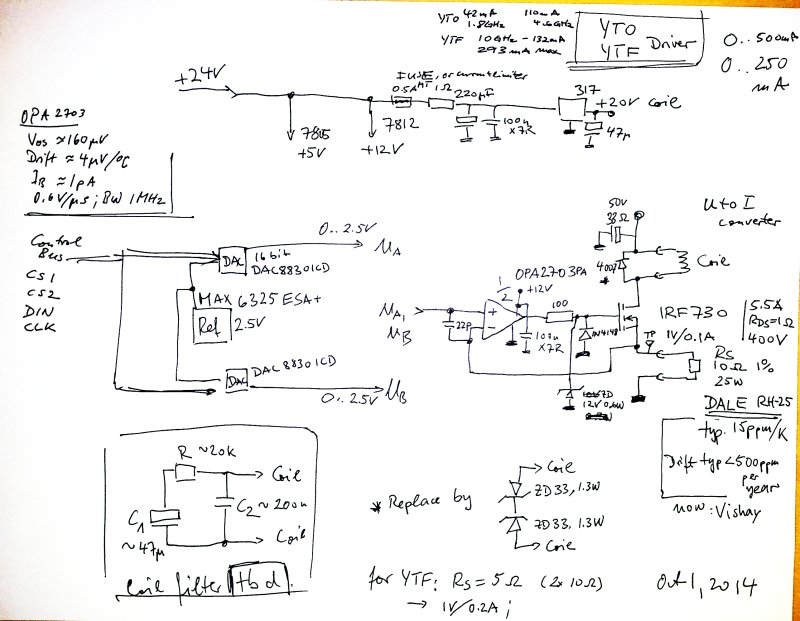
Well, after scratching my head for a while – and doing some measurements around the not-too-complicated 317 circuit, one 22 uF cap was added, to the adjustment input. Ideally, for best frequency response, use a low ESR cap, with wide response, like a tantalum or multilayer ceramic. I could not be bothered, just used a plain electrolytic.

Improved schematic:
msr pll power supply updated
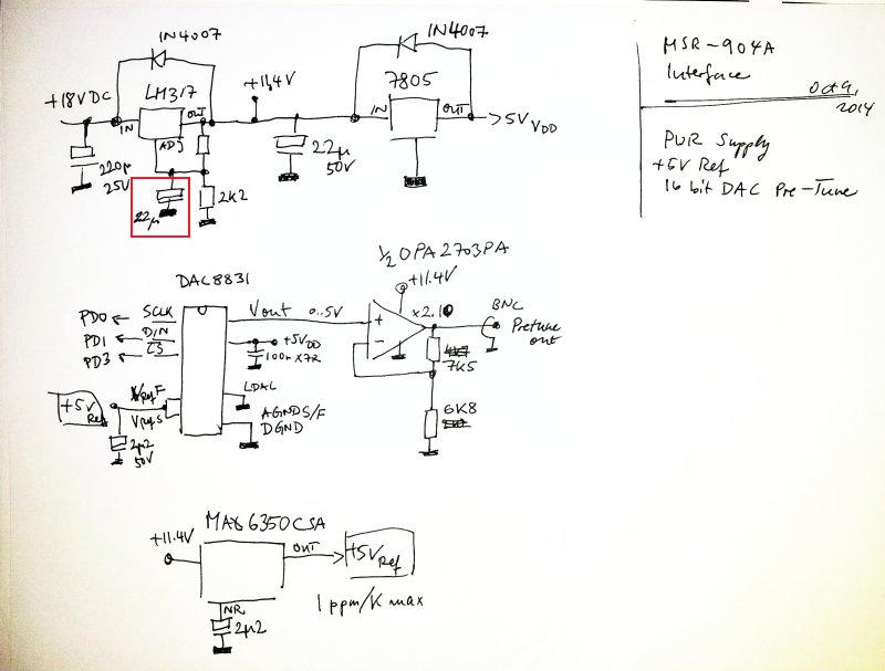
(red frame shows additional cap)

The result:
msr pll 317 noise 22 uf ref bypass 25k
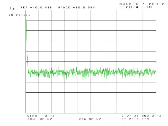
A 20 dB improvement, fair enough!

Step (2) – PLL low noise power supplies (2x 3.1 V)

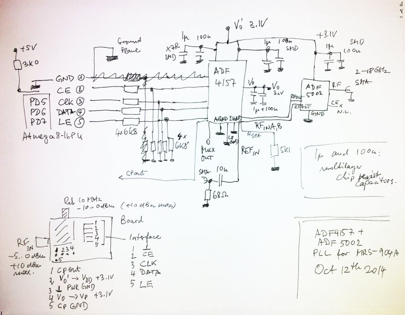
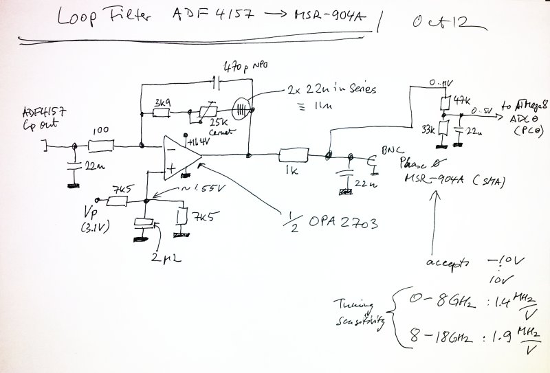
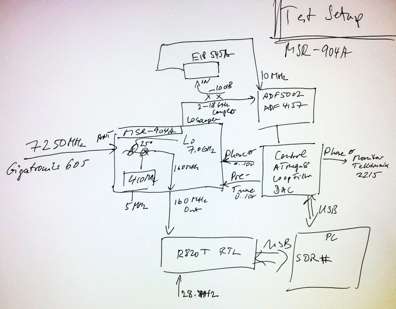
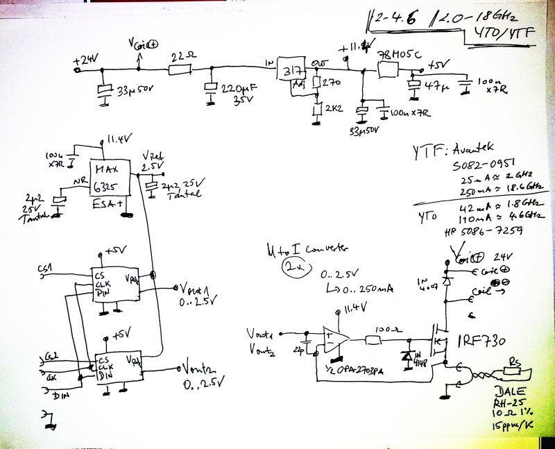
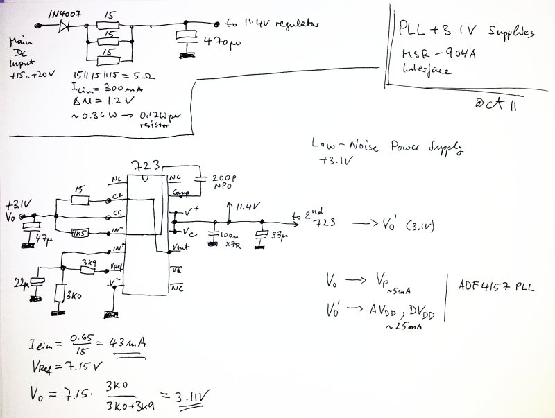
The PLL (an ADF4157 fractional-N synthesizer with ADF5002 prescaler) requires a +3.1 V power supply (2.7 to 3.3 V for the ADF4157, 3.0 to 3.6 for the ADF5002 – so I decided on 3.1 V for both devices). Also, we need a charge pump supply, for the ADF4157. This can be up to 5.5 V, but for simplicity of design, and to follow earlier (rather commercial) designs I did fully using 3.3 V technology, another independent supply is required, for 3.1 V.

These supplies need to very low noise, supply line noise will end up at the charge pump output, increasing phase noise. Glitches on the PLL supply lines can cause all kinds of issues, even the reliability of the circuit might be compromised (miscounting of the prescaler, etc.).

Quite a few more recent parts exist to provide about 3 V regulated output (see TI, Analog, LT), but these devices are non too widespread, and not much better, if not even worse than a trusty old part: the LM723 (aka µA723) regulator. This has a low noise reference build in, and should provide much better performance than any 3-pin regulator.

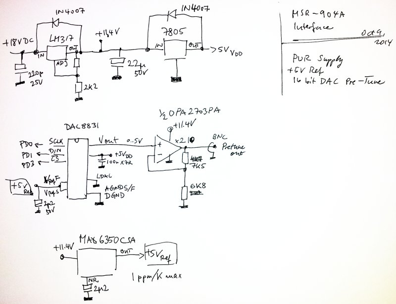
The schematic – main DC input, and 3.1 V low noise power supply section:
msr pll low noise power supply 3 volt

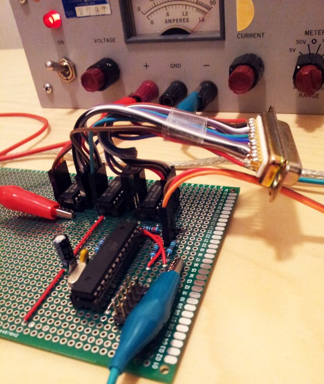
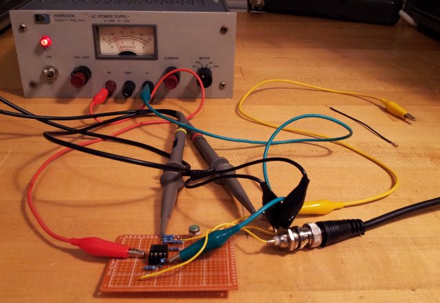
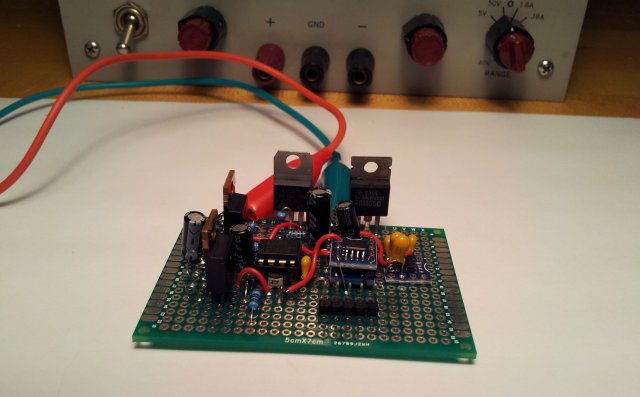
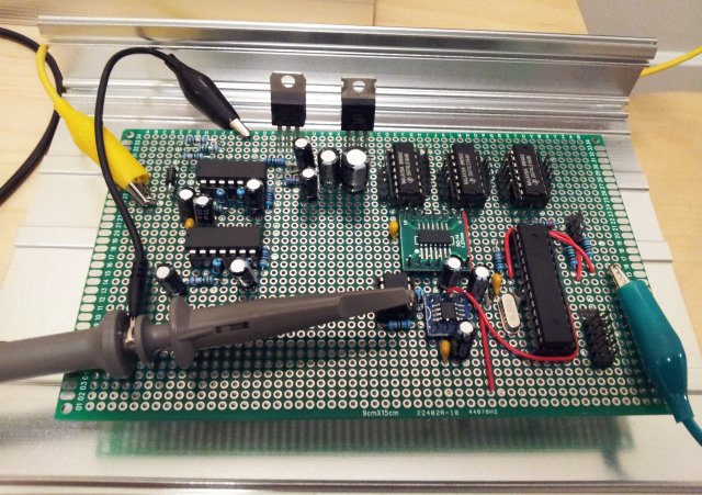
That’t the little board, during test:
msr pll test setup

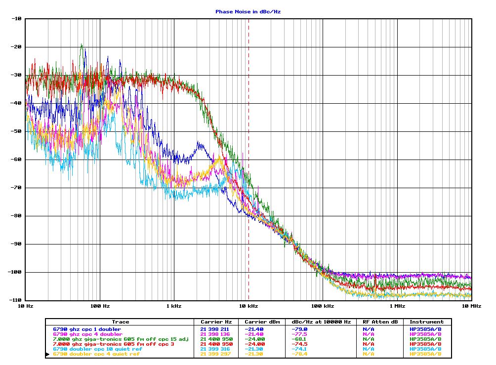
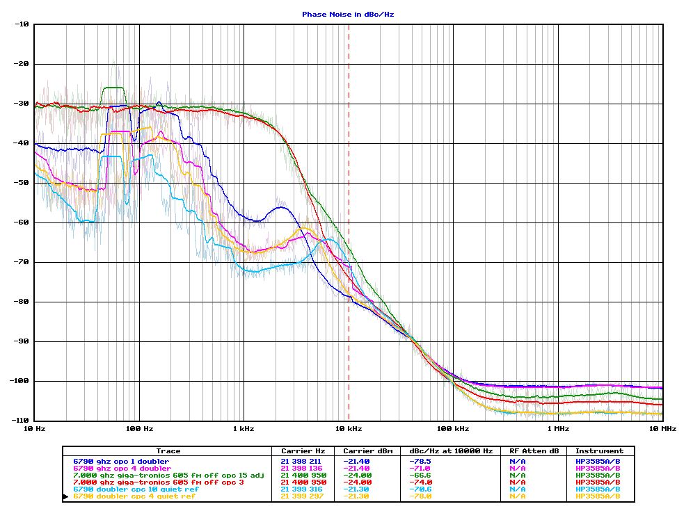
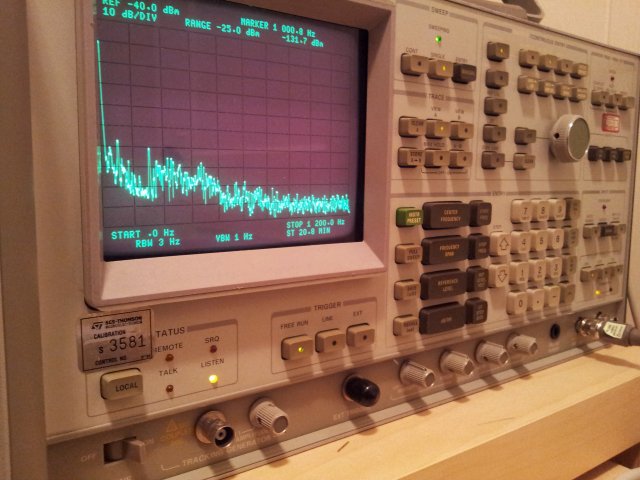
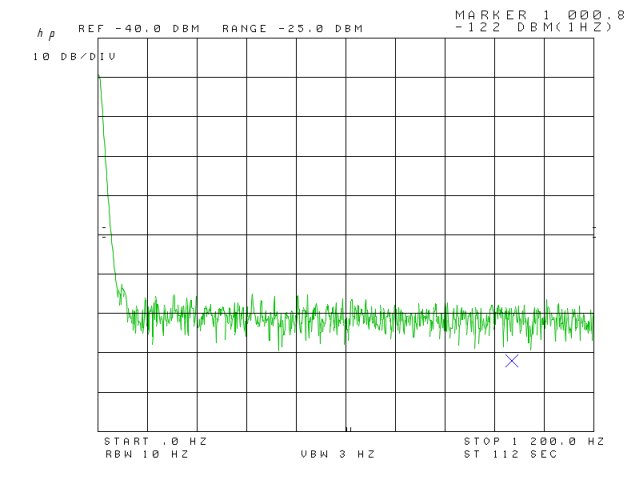
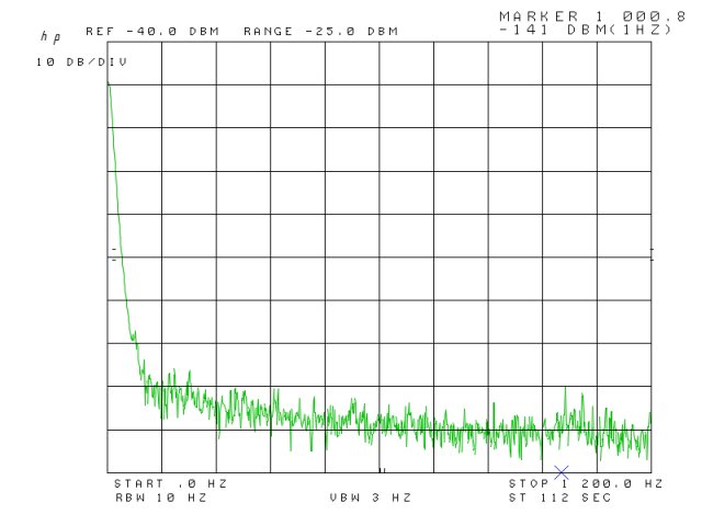
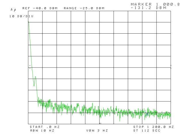
And here, we have the results – all tests now using 1.2 KHz stop frequency (not much going on at higher frequencies), 10 Hz resolution bandwidth, 3 Hz video bandwidth, and, using the noise measurement function of the 3585A – this directly measures and calculates the noise level, at a given frequency, for a 1 Hz bandwidth. Very handy for conversion to nV/sqrt-Hz (nV divided by square-root Hertz is a common way of expressing power supply noise).

Noise floor:
msr pll noise floor 1k2 grounded at agnd

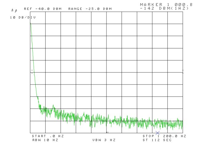
The 317 output (11.4 V) – supply of the pretune DAC circuit and amplifiers, and for the PLL active loop filter
msr pll 317 noise 1k2

The 7805 output (5 V) – digital supply, DAC supply
msr pll 7805 noise 1k2

The 723 output (3.1 V) – Vdd section
msr pll 732 vdd 1k2

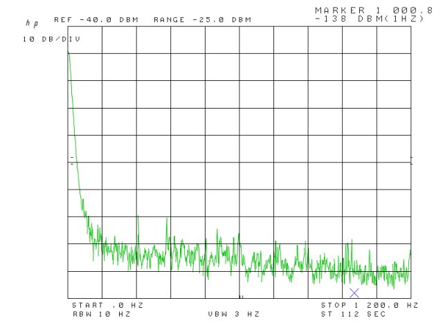
The 723 output (3.1 V) – Vp section (charge pump supply)
msr pll 732 vp 1k2

A converter worksheet, to relate the dBm numbers, to nV/sqrt-Hz (calculation also has provisions to convert from other bandwidth – not considering a few extra dB to account for the averaging nature of the detector, etc. – we rely on the 1 Hz normalized value of the 3585A anyway, just in case you need to convert from other BW, please keep dectector response related offset correction, if the task requires such levels of accuracy).
power supply noise calc 3585a

Converted values
-141 dBm – about 20 nV/sqrt-Hz (Vp supply) – very close to noise floor of the setup, the LM723 still seems good enough!
-122 dBm – about 180 nV/sqrt-Hz (5 V, 11.4 V supply)

Also, quick look at the DAC pretune output – at the OPA2703 scaling amplifier output:

msr pll dac amp vtune output 1k2
Virtually, below noise floor.

Note: there are some litte contributions at 60 Hz/180 Hz from mains. These are due to the test setup/signals picked-up by the test cables – don’t seem to originate from the circuit itself.

Micro-Tel MSR-904A Remote Interface: pretune DAC, precision reference, and some auxilliary circuit

Not a very exciting circuit today, but definitely, a very important one: the pretune DAC for the MSR-904A. This DAC will drive the 0..10 V input of the MSR-904A, to set the frequency for a given band. The frequency needs to be set to about 1 MHz or better, and the DAC needs to be virtually free of noise – any noise will be converted to phase noise, and cause a lot of hazzle for the PLL circuit to be added later.

Rather than a dual supply, the intention is to use a single +18 V supply for the whole remote control circuit. Therefore, we need a few linear regulators, to derive the +5 V for the digital circuits, including the ATmega8-16, and a positive voltage of about 12 V, for the analog circuit. The output driver for the pretune (0..10 V) uses an OPA2703 rail-to-rail opamp. So, I decided on a 11.4 V positive supply, for convenience of resistor values available – 270 Ohm, and 2k2, for a LM317 regulator.

The DAC, a Texas instrument DAC8831. A highly linear device – 1 LSB of INL error. Low noise, low power. The DAC is connected to a +5 V precision reference, a MAX6350. This is a pretty stable and low noise reference, very much recommended for 16 bit converters.

Well, not much more to say, here is the schematic:

msr-904a interface pretune circuit and power supply

And, a quick glance at the board:

msr-904a interface pretune and digital control

There is some space left on the board – for an ADC (to monitor signal strength), and for the PLL power supply (needs 3x 3 V, UA723 – for low noise), and a 10 MHz/5 MHz distribution circuit.

Reference Signal Conditioning: 10 MHz amplifier/limiter, :2 divider, 5 MHz output

A common task for most projects involving a PLL or other RF circuitry requiring a reference frequency signal is the conditioning of the incoming reference. These reference signals are typically very accurate in frequency, but never very accurate in levels, nor at the levels constant (sometimes, multiple instruments are connected to a single 10 MHz source, an disconnected when the setup is re-configured etc.). Also, there is always a risk of incorrect connection, with all these BNC inputs.

Therefore, we have a few requirements:

(1) Input needs to be stable to a reasonable DC voltage, say, a few Volts.

(2) Input needs to widthstand at at least 20-25 dBm input, about 0.25 Watts.

(3) Input needs to widthstand ESD, or other transients, and provide reasonable termination to avoid reflection. In the given case, we want about 50 Ohm – some reference inputs have higher resistance.

(4) Circuit needs to work from about -10 dBm on, up to 10 or 20 dBm, with no significant change in jitter, etc., and provide a stable, constant level output, TTL levels, or whatever is required.

The current circuit, which is intended to be a reference signal conditioner for a Micro-Tel MSR-904A Microwave Receiver, also needs a 5 MHz output – the PLL will run off 10 MHz, but the MSR-904A still is ancient enough to require 5 MHz (5 MHz used to be the standard reference frequency from early times up until the end of the 70s – since then, 10 MHz is almost exclusively used, and sometimes, 100 MHz, for double-digit GHz circuits).
Such 5 MHz output is easily realized by a divider circuit, based on a 74F74.

Now, how do we achieve all this. Well, here is the schematic:
ref signal conditioner schematic

The essential part – a 74HCU04. This little circuit is extremely useful – get a handful of these, they are not just “inverters” but acutally work at frequencies from DC to many MHz, can source and sink at least 4 mA to 5 V. The 74HCU04 is more or less a set of 6 push-pull MOSFET pairs, in a handy package. These pairs can also be paralleled with no precautions to get more current, if needed.

The signal input is protected by a 56 Ohm termination (which can burn out if you feed excess DC or more than 0.25 W of RF – unlikely to happen). Then, there is a 47 n decoupling capacitor, a series resistor, and a clipping circuit – which will most likely never be activated.
The 22k resistor, along with the first inverter, and the 470 Ohm resistor form the first amplifier.

Signal A (see letter on schematic, input of first inverter):
ref signal circuit A
-scope is set to 1 V per div vertical, 50 ns per div horizontal.

Output B:
ref signal circuit B

Note that the first gate is self-biased, no need to adjust anything.

This is then squared-up by the limiting action of the following 2 inverters:
ref signal circuit C

ref signal circuit 10 mhz E 1 v-div 50 ns-div

Now, we have a clean 10 MHz square wave. This is fed to a 74F74 edge-triggered flip-flop. The 74F74 is pretty fast, it easily works up to 100 MHz and will provide fast-rising edges.
The flip-flop will also ensure pretty much exact 50% duty cycle of the 5 MHz output.

ref signal circuit 5 MHz F

The output is fed through a low pass, 51 Ohm – 470 p, about 6.6 MHz, because we want low jitter at the divider stage (fast rise time pulses feeding the flip-flop), but not too steep edges at the output:
ref signal circuit G

After amplification by another 74HCU04 inverter:
ref signal circuit 5 MHz H
– this signal is still referenced to ground, and after another resistor and capacitor, finally, an AC signal, that can be used for various purposes, including frequency locking a MSR-904A.
ref signal circuit 5 mhz output I

Note: when you measure in such circuits, always use a >10 Meg, 10:1 low capacitance probe. Otherwise, you will get results, but these won’t reflect reality.

A quick test with a 10 MHz test signal – the circuit works well from about -22 dBm to 20 dBm, no issues at all. For the specification, and to ensure that is is working even under awkward conditions, we might limit it to -10 dBm to +16 dBm.

The little thing in action:
ref signal circuit test setup

Micro-Tel MSR-904A Microwave Receiver: remote control (digital interface)

The MSR-904A has a remote control interface, to control most of the front panel settings by TTL level signals – operation mode, band, filters, IF attenuator, detector. All in all, 22 signal lines are needed.
The circuit will also need provisions for latter addition of the PLL filter and PLL control – just a few digital lines. All will be controlled by a single USB interface.

First, we need a cable – the MSR-904A uses a DSUB-37 connector, but not all pins are used – so an adapter cable was fabricated to convert this to a much more common (and available) DSUB-25:
msr-904a remote control cable
– quite a few wires!

msr-904a remote interface wiring and register layout

The digital control is implemented by a set of three 74LS164 shift registers, serial in, 8 bit out. These registers are very fast, can be set in a few microseconds. The three registers are named 1-Q0 (LSB of register 1) to 3-Q7 (MSB of register 3).
The micro is an ATmega8-16PU, running at 16 MHz – this has plenty of power to handle the USB interface, the digital control, and later, the PLL loop. There is also a standard 10 pin ISP header, not shown in the schematic.

msr-904a digital interface schematic

The circuit – build on a perfboard. No plans to fabricate a PCB, I don’t anticipate a big demand for MSR-904A remote control units, but still it should last many years. This is why a proper FR4 perfboard with plated-through holes is used.

msr-904a digital interface

HP Fundamental/Harmonic Mixer 5086-7285 (22 GHz): digital bias control

In an effort to build a 2-18 GHz down converter, a HP mixer 5086-7285 needs to be controlled. This is one of a group of 22 GHz mixers, all used in earlier HP spectrum analyzers. These mixers are very linear, and useful both at fundamental and harmonic frequencies.

That’s the little magic thing, and the frequency list-harmonics:
5086-7285 mixer
5086-7285 mixer harmonics

All in all, at a first glance, pretty easy to use – it only needs +10 and -10 V power supply and bias for the diode.

Well, bias, after looking through the schematics, this is the assembly taking care of it: a board full of resistors and amplifiers, with no less than 22 (!) adjustment pots.
08565-60023 bias assembly

The interesting part are the bias drivers itself –
hp bias circuit for harmonic mixer
– the linearization, etc., this can all be done easily by using digital memory and a DAC nowadays, but the drivers, we still need them.

The bands B3 and B5, the even harmonics, the things are clear and as expected – a voltage source, and a resistor. Easy enough. But, what did HP do for the odd harmonics?? – the are a few extra resistors around the opamps, and these resistors make it a tricky thing. Too tricky to make it easy to understand. Some kind of negative resistance circuit/kind of a voltage to current converter, which depends a bit on the load resistance.

So, what do you do to understand such things better – build a little test circuit, here we go:
mixer bias test circuit
-it is essentially the same circuit, as for the B1/B4/B2 bands, U6B of the HP circuit- just left out the switching transistor.

It works pretty well, and as a U to I converter, see here:
bias driver test 200 mv-div ramp  1 mA-div current
– ramp voltage is the drive signal, 800 mV p-p, 200 mV per div (center line is zero). During the negative signal period, the output is active – current signal is 1 mA per div (center line is zero).

Having the basic functionality of the ciruit confirmed – some calculations with LTSpice, one of the best general purpose analog simulators around, Thank You, Linear Technology!

Here the files, in case you want to investigate it yourself:
hp mixer bias

This is a typical result, mixer bias current, vs. input voltage of the circuit, at resistance (of the mixer), of 950 (steepest)-1050-1150-1250 ohms.
r6-92 1-9 bias rscan vs Vi
So, this cirucit really is a U to I converter, with the slope depending on the load resistance.
Also note the model circuit of the mixer internal resistor and diodes. The two diodes and the 970 Ohm resistor are the result of bias current vs. bias voltage measurement. Bias voltage is in the range of -1 to -7 volts, about 0 to 8 mA.

With these findings, next step will be to build a driver circuit that can work fully digitally controlled, with no adjustment pot at all (series resistors will be manually selected).

YTO YTF Driver: 0..250 mA, 16 bits resolution

Quick update on the YTO/YTF driver board – with 16 bits of resolution. Assembly, is complete, and basic function has been checked – digital control test will follow tomorrow.
Current is settable from 0 to 250 mA, with 65535 counts of resolution – about 3.8 Microamps per LSB. All has been build to minimize noise, with heavy filtering on the supplies. The DAC is run from a dedicated 5 V supply, with a 2.5 V precision reference, 1 ppm/K, MAX6325ESA+.
The U to I converter is powered by 11.4 V – provided by a LM317 voltage regulator.
Switching element is an IRF730, operated as a series variable resistance in series with the coil.

YTO YTF driver 2x250 mA 16 bit

YTO YTF driver 2x250 mA 16 bit schematic

Looking at the BoM, the parts sum up to about USD 35 plus board, not bad – target is to stay below about $100 for the final assembled unit, which will be achievable, no issue. Main cost comes from the MAX reference, and the DACs (DAC8830), almost USD 22.

To come: bandwidth testing

YIG tuned oscillator (YTO) / YIG tuned filter (YTF) driver: digitally controlled current source

For a digitally controlled YIG oscillator and filter, a driver is needed that can convert serial data from a microcontroller to a well defined, stable, and low noise current.
Bandwidth of the circuit should be a few 100 Hz, and maximum current in the 300 mA range, so it needs to run of a reasonably high supply voltage, otherwise, the inductance of the coil will limit the slew rate. The YTO needs about 120 mA full scale, the YTF about 260 mA.

I might do some fine tuning on the DACs later or change the current sense resistors for a 2.5 V drop at close to max current, for best signal to noise ratio, but for the test circuit, 10 Ohm RH-25 resistors will be used. The current sense resistors are a very critical part – they need to be low drift, over time, and over temperature, regular resistors, with 100 ppm/K or more will only cause drifting frequencies, and trouble.

Here, the draft schematic, as-build:
YIG driver schematic dac control - u to i converter

That’s the test setup, with +20 V and -10 V power supply, for the YIG. In the final setup, there will be independent, filtered and regulated supplies for low phase noise.

YTO driver test setup

The circuit is driven by a HP 8904A signal generator, with independent adjustment of offset and voltage. Here, the output at 70 mA current, with a +-1 mA amplitude variation:

YTO output 70 mA +-1 mA
YTO is a HP 5086-7259, 2.0-4.5 GHz (nominal).

So, about +-40 MHz – close to expected +-35 MHz.

Bandwidth analysis will follow.

Here a quick calculation of the DAC resolution, 1 LSB will be about 0.13 MHz, more than sufficient for the DAC tune. The DAC used, a DAC8830ICD has typical +-0.5 LSB non-linearity, max +-1 LSB. Additional tuning will be easily accomplished by the FM coil, using a PLL.

yto ytf dac calculator