Many design of amateur noise sources have been published, they all have there benefits and shortcomings, but it is mostly the lack of a calibrated test source that makes it difficult for the hobbyist to employ a cheap, home-made noise source for the ever-so-critical noise figure measurements of the amplifiers and mixers he may build.
Having recently acquired a good calibrated source, HP 346B, I have decided to make available a noise source design and build so many, and calibrate them, in order to make calibrated sources, up to, say 1.5 or 2 GHz, available for everyone at a really low price. Thinking about USD 45 per piece which should be fine for everyone dealing with such measurements.
Requirements are pretty simple, it should be a ‘low-frequency’ replacement of the HP 346B, about 15 dB ENR output, flatness, preferably, within 0.5 dB, starting from 10 MHz. It should also have high output return loss (low SWR), which can’t change significantly from on to off state. Last but not least, powered by the ubiquitous 28 VDC noise source drive signal common to most noise figure analyzers.
The bill of materials, combined with the desired target price, won’t allow the use of a custom-made noise diode. But this is not really a disadvantage for the intended frequency range and purpose.
Three main tasks will have to be solved, to get this thing (called, the TWS-N15 Noise Source) to work:
(1) First and foremost, we need a noise generator circuit; these require a bias current, typically 5-15 mA.
(2) We need a temperature-compensated current source; currently experimenting with discrete Zener and TL431 based circuits. Current should not vary significantly, if input voltage is changing from, say, 27.5 to 28.5 VDC.
(3) Mechanical package. This is quite important, because the noise source needs to be well shielded, and put in a sturdy case – these sources tend to float around labs, and are often dropped, or dragged down from the bench by the heavy cables attached. Output connector will be SMA, because I have a large supply of really nice quality SMA print connectors.
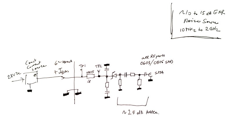
The draft schematic (current source not shown, cirucit works, but still need better characterization, and possibly, some improvement). Note that the output attenuator will set the ENR level. Might need to adjust this a bit; for the time being, anything from 10 to 15 dB ENR will be fine.
This is the small cirucit, build on a 0.6 mm FR4 board. Traces were simply carved out with a knive…..
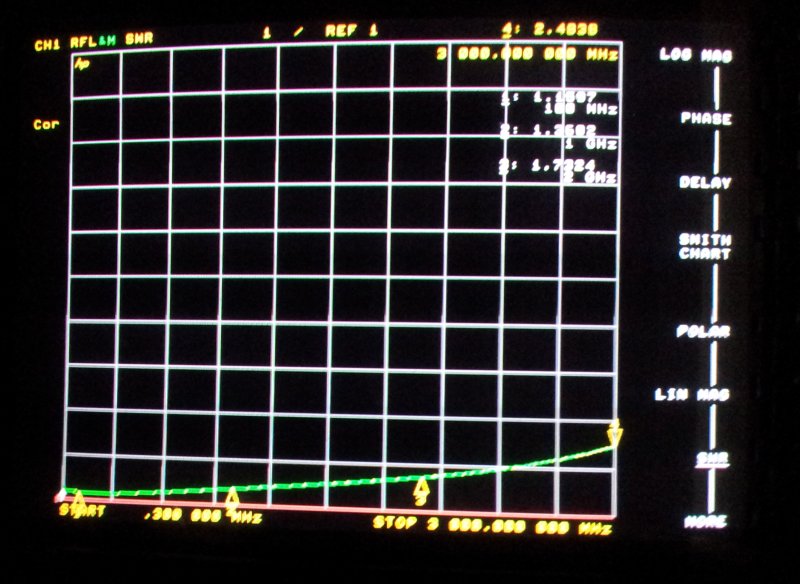
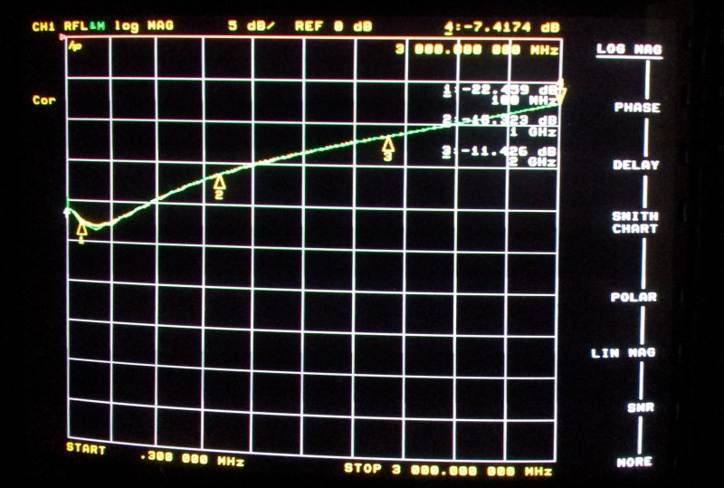
Here a few plots from the VNA characterization. Not bad for a start. Input return loss is at least 15 dB. This will still be improved. Using 0603 SMD resistors for the critical section.
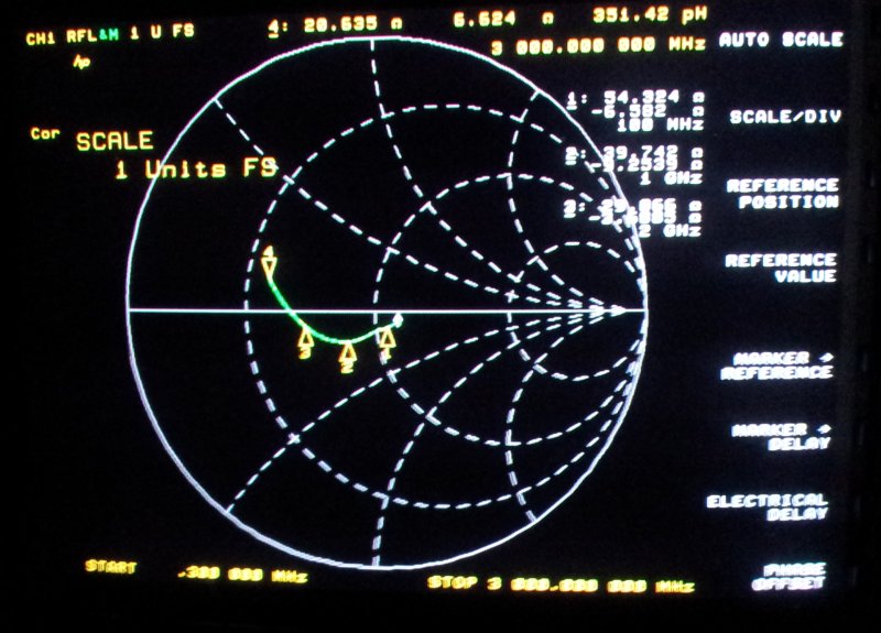
ON and OFF traces are shown – virtually, no effect on the return loss.
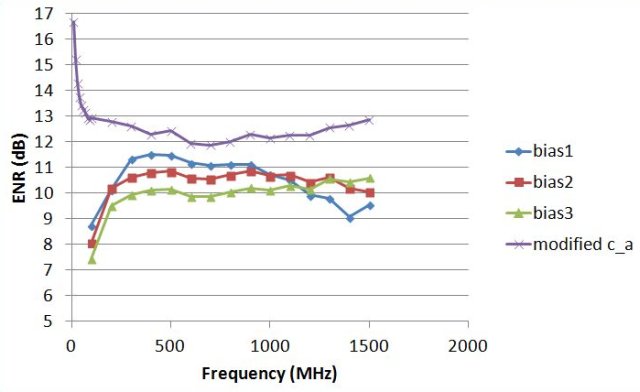
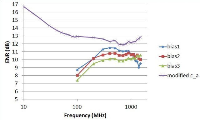
Some tests of the noise output, really much better than I thought. Bias current has some impact on flatness; low frequency end is determined by the first capacitor (between diode and attenuator). This will need some further tweaking to get it as flat as possible, but no rocket science.
To measure the noise output flatness and level quickly, there is no also an automated test rig here, which measures bias current and on-off noise figure differences.
Next steps… will need to decide if the 0.6 mm board is the best option (these boards allow rather narrow 50 Ohm traces; most of them, I machine using a router mill – no etched traces), or if a commercially made board of regular dimensions would be the better option. Cost ist not really a concern, because the noise source only needs little space. Stay tuned.

