All posts by Simon

TWS-N15 General Purpose Noise Source: some progress on the design, and some tests

Many design of amateur noise sources have been published, they all have there benefits and shortcomings, but it is mostly the lack of a calibrated test source that makes it difficult for the hobbyist to employ a cheap, home-made noise source for the ever-so-critical noise figure measurements of the amplifiers and mixers he may build.
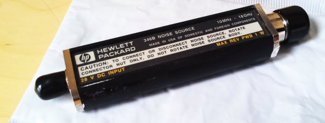
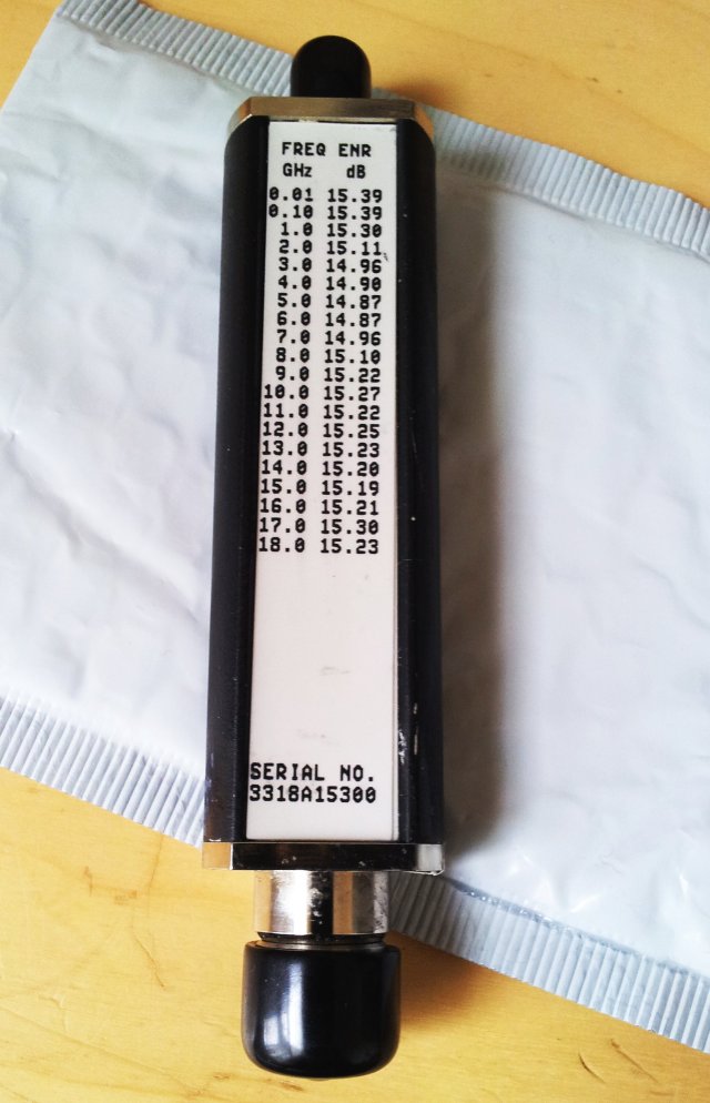
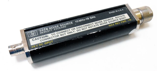
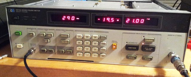
Having recently acquired a good calibrated source, HP 346B, I have decided to make available a noise source design and build so many, and calibrate them, in order to make calibrated sources, up to, say 1.5 or 2 GHz, available for everyone at a really low price. Thinking about USD 45 per piece which should be fine for everyone dealing with such measurements.
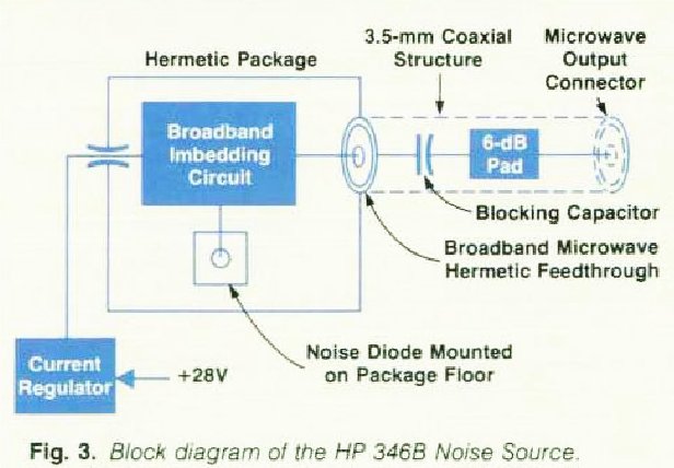
Requirements are pretty simple, it should be a ‘low-frequency’ replacement of the HP 346B, about 15 dB ENR output, flatness, preferably, within 0.5 dB, starting from 10 MHz. It should also have high output return loss (low SWR), which can’t change significantly from on to off state. Last but not least, powered by the ubiquitous 28 VDC noise source drive signal common to most noise figure analyzers.

The bill of materials, combined with the desired target price, won’t allow the use of a custom-made noise diode. But this is not really a disadvantage for the intended frequency range and purpose.

Three main tasks will have to be solved, to get this thing (called, the TWS-N15 Noise Source) to work:

(1) First and foremost, we need a noise generator circuit; these require a bias current, typically 5-15 mA.

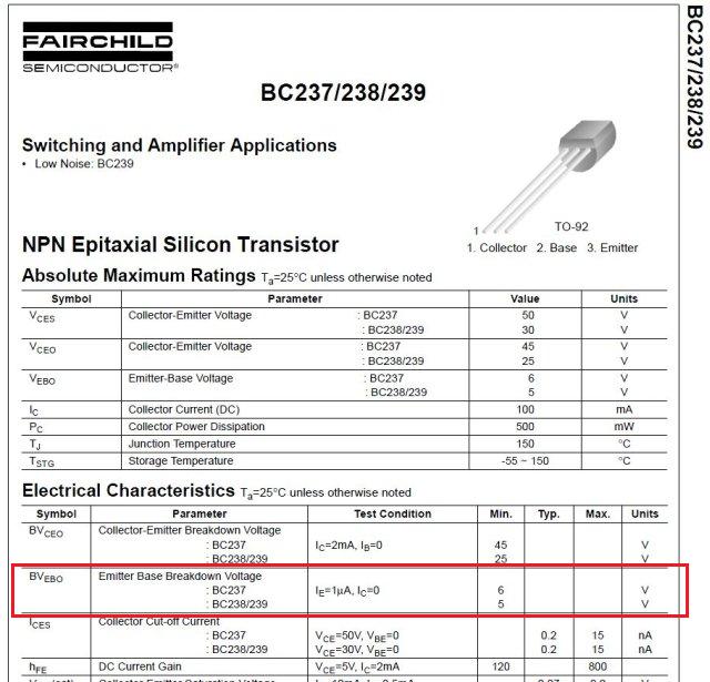
(2) We need a temperature-compensated current source; currently experimenting with discrete Zener and TL431 based circuits. Current should not vary significantly, if input voltage is changing from, say, 27.5 to 28.5 VDC.

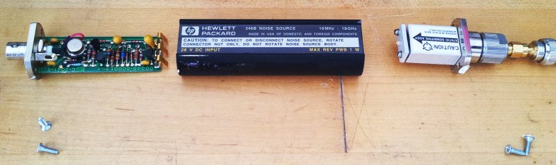
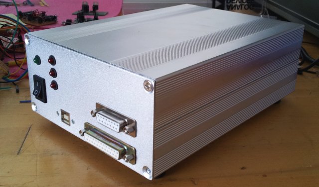
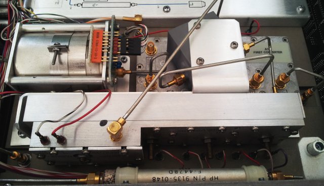
(3) Mechanical package. This is quite important, because the noise source needs to be well shielded, and put in a sturdy case – these sources tend to float around labs, and are often dropped, or dragged down from the bench by the heavy cables attached. Output connector will be SMA, because I have a large supply of really nice quality SMA print connectors.

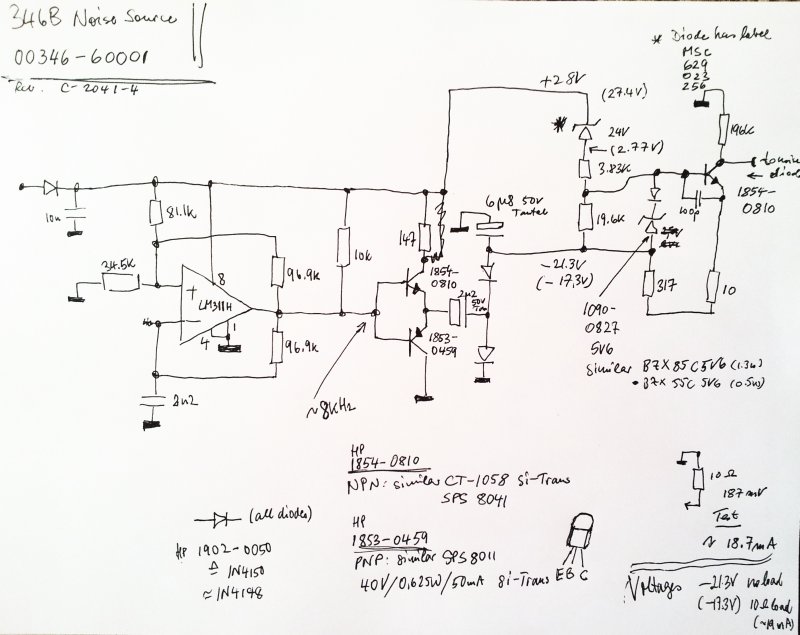
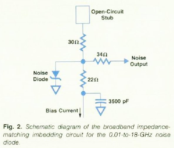
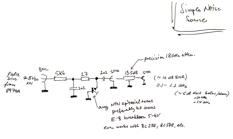
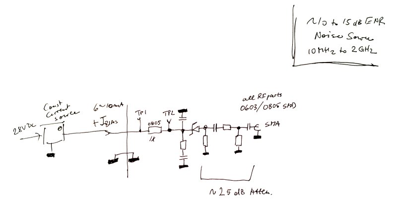
The draft schematic (current source not shown, cirucit works, but still need better characterization, and possibly, some improvement). Note that the output attenuator will set the ENR level. Might need to adjust this a bit; for the time being, anything from 10 to 15 dB ENR will be fine.

tws noise source schematic

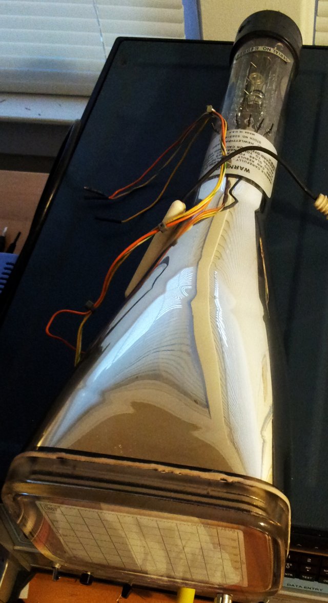
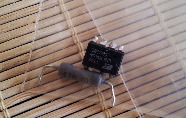
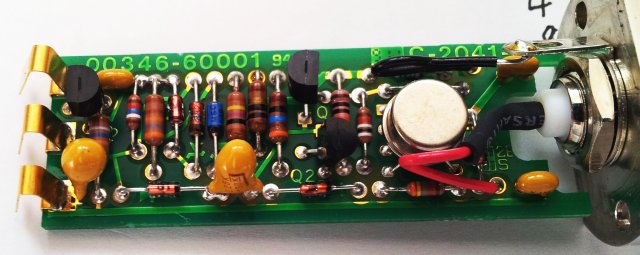
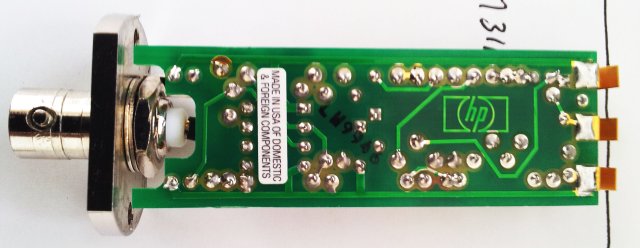
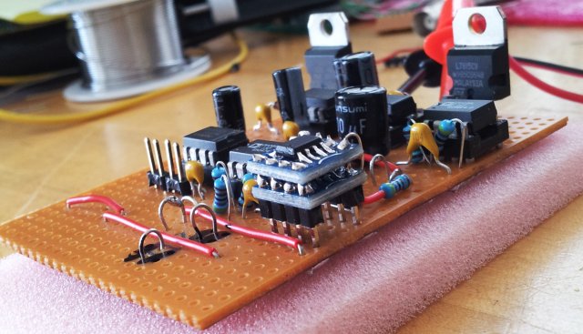
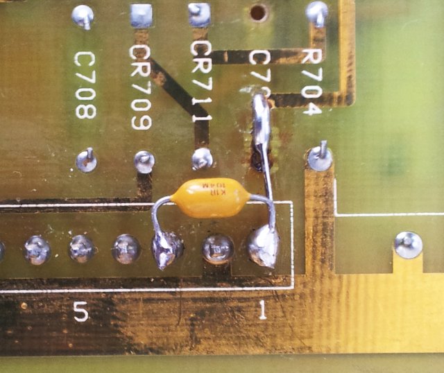
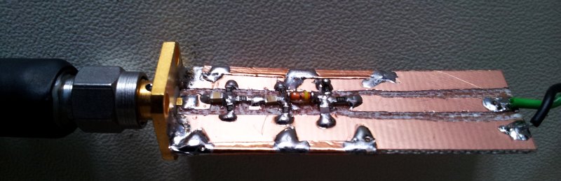
This is the small cirucit, build on a 0.6 mm FR4 board. Traces were simply carved out with a knive…..

2 ghz noise source

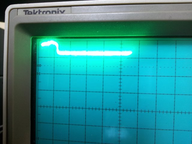
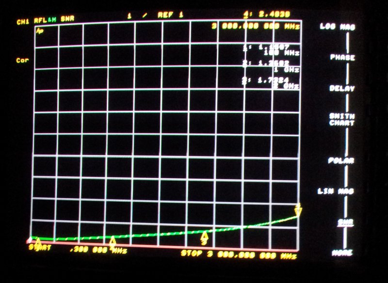
Here a few plots from the VNA characterization. Not bad for a start. Input return loss is at least 15 dB. This will still be improved. Using 0603 SMD resistors for the critical section.
tws noise smith chart

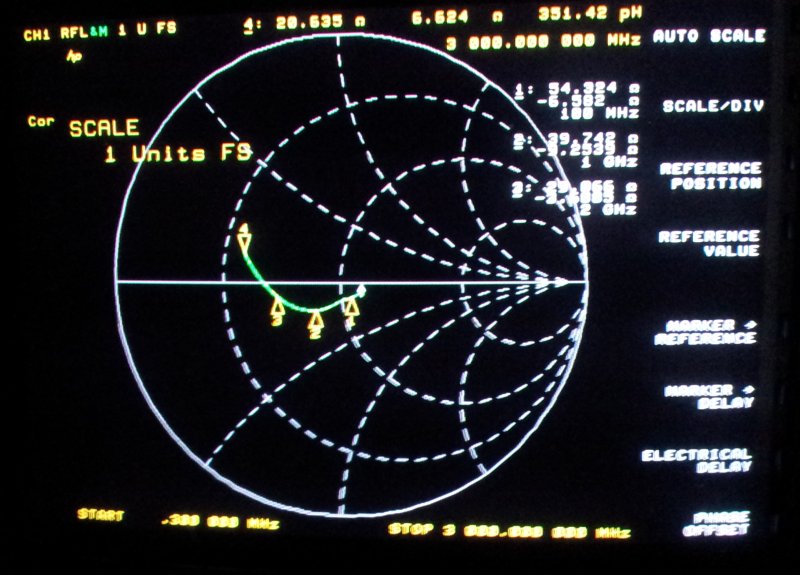
ON and OFF traces are shown – virtually, no effect on the return loss.
tws noise rfl loss on off

tws noise swr

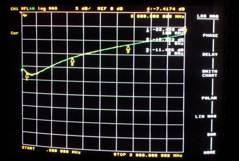
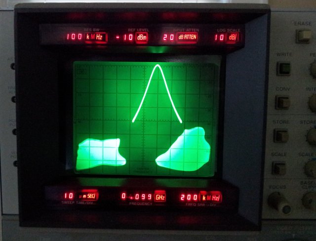
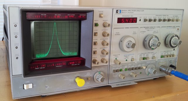
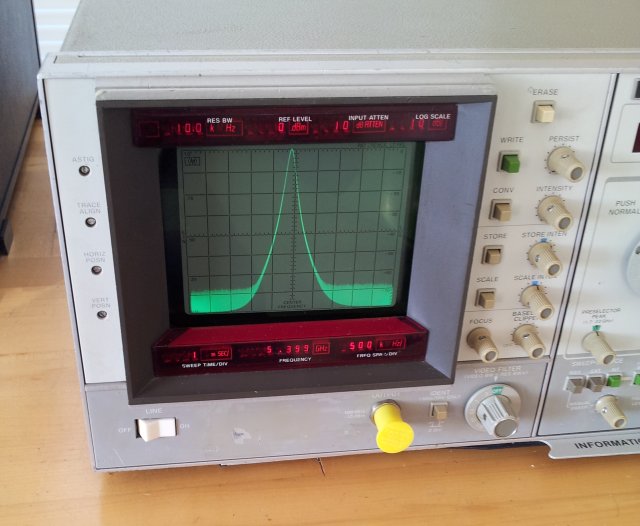
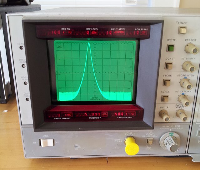
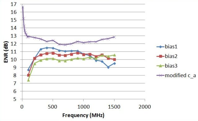
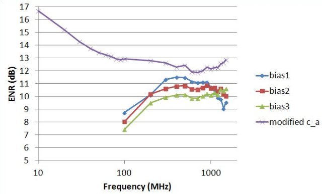
Some tests of the noise output, really much better than I thought. Bias current has some impact on flatness; low frequency end is determined by the first capacitor (between diode and attenuator). This will need some further tweaking to get it as flat as possible, but no rocket science.
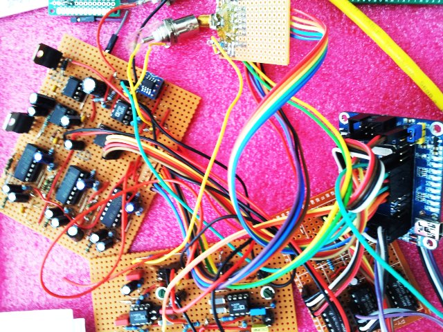
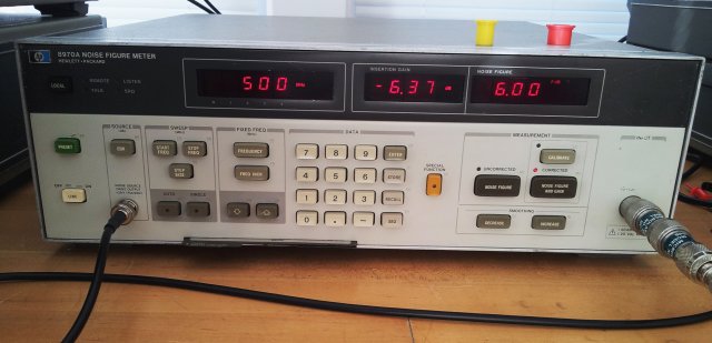
To measure the noise output flatness and level quickly, there is no also an automated test rig here, which measures bias current and on-off noise figure differences.

noise source test1

noise source test1 log

Next steps… will need to decide if the 0.6 mm board is the best option (these boards allow rather narrow 50 Ohm traces; most of them, I machine using a router mill – no etched traces), or if a commercially made board of regular dimensions would be the better option. Cost ist not really a concern, because the noise source only needs little space. Stay tuned.

HP 8565A Spectrum Analyzer: a ‘new’ CRT for a trusty unit

Not a very major repair, but certainly, noteworthy. I have a 8565A here on the bench, and actually use it quite a lot, along with the 8569B, because it saves you a lot of time not to have to wonder about all the buttons and switches of more sophisticated analyzers. Also, for its coverage (up to 22 GHz with no external mixers), it is rather affordable, and should it suffer from accidental abuse, which can always happen on a test bench with so many cables, it is rather easy to fix because of parts units being available, and because of its discrete construction. Needless to mention, full schematics are available from the HP service manuals.
The only downside of the unit, the CRT – it is working just fine, for all practical purposes, but has some ‘slow’ sections in the variable persistance and storage modes. These show up as green spots in the baseline region. Over time, you can make them disappear, but it takes multiple erase cycles, quite a tedious procedure. For the most part, I just did not care about these spots.

8565a old crt

Fortunately enough, I was able to get hold of a spare 5083-4471 CRT, which has been sitting in the storage room for quite a while. Condition was said to be ‘essentially new’ but never checked.

crt 5083-4471

8565a crt screen

8565a new crt

Last week, finally decided to give it a try, risking to have to install the old CRT again, in case the new one doesn’t turn out to be so new.

You be the judge…. conventional mode

8565a crt conventional mode

… stored display …

8565a new crt storage

… variable persistence mode …

8565a new crt variable persistence

…. good as new.

Clothes dryer repair: AKO 742336 control unit type EDR0692XAX

Repairs of household appliances aren’t generally my field of expertise, but in some cases, it can be a very rewarding activity. Some particular models of clothes dryers (“AEG”, “Whirlpool”) common in Europe use a control board, and this is not designed up to standard. The design flaw, it renders the machine inoperative in the very sense, you can’t switch it on, and it doesn’t show anything on the display. Typically, this occurs after roughly 3 years of service….

This is the control unit:
dryer control

dryer control board

dryer control board detail

edr0692xax board

After a quick inspection, it is fully clear that the defect rests with the control board, model EDR0692XAX. Easy fix, just get a spare! Well, easy, but outrageously expensive.

ako 742336 edr0692xax

The defect, it is related to a DC switch mode regulator converting mains voltage down to some useful voltage to run the controller. This is a step-down converter, NOT mains insulated!

lmk304 application

Two dead parts were found, the LNK304 switch mode converter circuit, and a 47 Ohms resistor.

dryer control lnk304gn 47r resistor

The LNK304GN is easily found, and replaced. The resistor: WATCH OUT! This is a fusible resistor, NEVER replace with just a common resistor – it will potentially set your house on fire, when the next switch mode failure happens.
The 47 Ohm resistor, it’s a 3 Watt resistor, and the ULW3 series, available from all major suppliers, should be a good replacement.

ulw3 fusible resistor

This is the failure charcteristics of the ULW3 resistors – it will go open circuit if overloaded, without release of any flames or particles. It a hybrid, partly fuse, partly resistor.

ulw3 fusing characteristics

USB RTL SDR 28.8 MHz Reference: VCO design established

A quick update on an earlier post, USB RTL SDR 28.8 MHz Reference: VCXO, development of a low-noise 28.8 MHz is now complete. A BB159 varicap has been selected for the voltage tuning control, and it works nicely, even within a 10 V tuning range. This is a UHF varicap diode, C_28V of about 2.1 pF, 9:1 ratio.

bb159 varicap

The updated schematic – the test setup still shown here still uses a few through-hole parts, put most of the RF caps are SMD 0805. J310 J-FETs are used, both for the oscillator, and the amplifier – mainly because of their low cost, and they are widely available.

28800 vco schematic

This is the test setup – test signal provided by a 8904A, and frequency measured by a 5372A Time and Frequency Analyzer, 4 s gate time.
28800 vco test

That’s the tuning curve, it happened to be at 28.800000 MHz, for about 5.5 Volt, nicely centered within the tuning range. No need to worry about the deviation from linear slope, the PLL will have a very long time constant, and the non-linearity of the tuning curve won’t have any impact on the VCO performance.
28800 vco tuning curve

A nice additional feature – this VCO circuit works with the default 28.8 MHz crystal (which is actually no so bad, it is quite stable over temperature, at least the samples I have tested here, taken from cheap USB RTL SDR sticks). +-700 Hz range, +-25 ppm, should be pretty much sufficient to keep the VCO locked over a wide range of temperatures. If not (for other 28.8 MHz that might be around out there), two of the varicaps can be used in parallel, and the C* capacitor adjusted a bit; pullability of the xtal is pretty good, +-1.8 kHz is easily possible. It is best not to use a trimmer cap, but to solder-in suitable capacitors, to keep noise down, and stability up.

HP (Agilent Keysight) 346B Noise Source: finally, a calibrated ENR standard, and a temperature compensated current source

Today, a rather ordinary envelope arrived, still it feels a bit like xmas, because of the contents….
346b envelope

…. a HP (Agilent Keysight) 346B Noise source, with nominal 15 dB ENR. I have long been looking for one, at a reasonable price, and finally scored this unit on xbay.

346b

The calibration sticker shows good flatness, especially, in the 0.01-1 GHz region, which I need most, it is perfectly flat.

346b enr cal

Prior to having it re-calibrated, a good opportunity to look inside. There are two sections: the current source, and the RF noise source assembly (which is hermetically sealed, and you better don’t touch!).

346b parts

These are some close-ups of the 00346-60001 power supply and current regulator board.

346b top side

346b bottom side

The current regulator inside of the 346B has always been a big mystery to me, because no schematic has been published by HP, in any of the service manuals. How it works, check out the schematic. The incomming 28 V (which is provided by the noise figure meter) is converted to a square wave, about 7-8 kHz, using a LM311H comparator. This is then converted to a negative voltage, about -20 V, absolute value varies a bit with loading condition.
The negative voltage is then used to sink current from the noise source assembly. The current setting of my unit is about 18.7 mA, programmed by the “10 Ohm” resistor.
Why the negative voltage? To simplify the design of the noise diode.

00346-60001 346B noise source schematic

Why did HP use a 5V6 Zener for the current reference, well, this is fairly obvious, when looking at the datasheet of such diodes.

bzx85 zener data

Around 5.6 V, the temperature coefficient virtually vanishes (this is why such voltages are also used for voltage reference circuits). The other Zener diode, unfortunately, I was not able to identify. It has 24 V drop, fair enough, any regular Zener should to the job to keep the base bias of the output constant.

For a quick burn-in, the source has now been connected to a 8970A Noise Figure Meter, and output appears to be very steady, less then 0.1 dB drift over a few hours. More noise measurements and calibration tasks to come, let me know if you need any noise sources measured, might be able to help.

Latching Coax Relais Driver: useful for all kinds of HP/Agilent/Keysight attenuators and switches

Driving a latching relais doesn’t sound all that complicated, and it isn’t, still, some thought is needed to get it working properly. This is what the circuit should do

(1) Accept one 5 V TTL input signal, LO signal will result in the relais switched to the rest position, HI signal to the activited position (“dash” position), the switching signals are called A and A’, for relais A.

(2) There should be an output-enable signal for all relais, to be able to de-energize the relais, because otherwise, the circuit can suffer if the relais is disconnected while powered; these latching relais only need a few 10s of Milliseconds to switch, power will be turned off, by the ATmega32L, 1 sec or so, after each switching event, just to avoid any unintentional short circuit or spike, and the positive supply line will carry a fuse.

(3) The circuit should be able to handle any common relais voltage, 5, 12, 15, 18, 24 and 28 V. The relais I am using here are 24 V rated, but work fine at 18-20 V, and up to 28 V.

(4) It must be avoided, at all cost that both the A and A’ signals are active at the same time. This can cause nasty relais oscillation, and damage/wear of the expensive relais. We don’t want to rely on software control here, because things can go wrong, during startup, program freeze, and so on.

coax relais driver schematic

The circuit is almost self-explanatory. The LS04 generates the complementary control signals, from the digital input. The LS373 is configured as a transparent latch, in fact, the latch function is not used, but the output control function is. If the OC input goes LO (and thus, the neg_OC high), the outputs of the LS373 will tri-state High-Z.

The output driver, a Toshiba ULN2803APG is used. These are very reliable circuits, Darlington transistor arrays with build-in diodes.

uln2803apg

Make sure to put a good quality capacitor close to the COM pin, the return path for the snubber diodes, otherwise, the inductance of the traces will deteriorate the action of the diodes. Actually, the HP coax relais have build-in diodes, so I don’t expect and issues with voltage spikes here.

Note that the inputs of the ULN2803 have adequate resistors to ensure LO state when connected to a High-Z output; if other transistor arrays are used, the circuit might need some ~10 kOhm pull-down resistors to ensure noise immunity and defined signal levels.
The 15 kOhm input resistors serve the same purpose, they keep the relais de-energized if no logic input is connected.

This is the little board, with all space well used. Sure the logic could build using more modern devices, and I would definitely do so for a commercial device, or anything build in series, but LS logic is still popular, and it is cheap, at hand, and reliable.

coax relais board

That’s the setup, with the two 8673B transfer switches, and a 0.3 Hz test signal fed to the digital inputs by the brown wire shown above (removed for the picture below).

coax switch setup

The signal at one of the contacts, 24 V drive level, 1 V per vertical DIV, 10 ms per horizontal DIV. No spikes, high voltages, or similar undesirable features are present.

coax switching

After about 2000 switching events, two events per 3.3 seconds, everything is still working well, and all circuits, in particular, the ULN2803 stays cool.
As I said, not a very complex circuit, but may be useful for other purposes, and is a very cost-effective, reliable solution.

Tripple PLL Controller, for Micro-Tel SG-811/1295/1295: converting a ratsnest to a shiny box

Comming back to an earlier project, the frequency stabilizers/PLL controls for the Micro-Tel 1295 receiver (2 pcs, one for through, and one for reflected power), and the Micro-Tel SG-811 generator (0.01-18 GHz).
The setup has been working well, but it is an awful mess of cables, as a result of the development process.

18 ghz pll wire mess

Now is a good time to finalize the circuit, and to put it into a nice case.

pll controller case

This is the front panel – the back panel has numerous BNC connectors, for the “PLL Phase Lock” voltage, and the “Frequency Control”, i.e., coarse tune voltage. The latter voltages, 3x 0-10 Volts, are generated by a DAC board, which is now ready and tested. Not a thing of beauty, but it works, and no reason to assemble another one just to clean things up a bit.

dac board

The circuit is reasonably straightforward, a 2.5 V precision reference is used, and three MAX541 16 bit DACs, followed by OP284 amplifier to convert the signal to the 0-10 V range.
The MAX541, it’s a really great part, full 16 bits, +-1 bit integral nonlinearity, and very stable over temperature and time. Highly recommended for any precision application.
One of the channels has an additional TLC2201 opamp, which is there more for historic reasons than for anything else.

dac board schematic

The PLLs use three ADF41020 18 GHz chips, following the approach discussed earlier. This will give 100 kHz frequency resolution, which is more than sufficient for the intended purpose of measuring gain/attenuation and SWR over the full range of microwave frequencies up to 18 GHz, or 40 GHz, if no SWR measurement is required.

The 10 MHz reference circuit has also been completed, and is working well, converting a 10 MHz input signal (of more or less arbitray shape and amplitude) to 3x 10 MHz REF signals for the ADF41020, and two 5 MHz outputs, for the 1295 receivers, just in case I need to work with external downconversion-the 5 MHz signal is only affecting the 0.01-2 GHz range of frequencies. Well, why not having everything phase locked, if we can.

10 mhz 5 mhz ref circuit schematic

The 10 MHz circuit has been modified slighly, to accept 1 kOhm impedance 10 MHz input signals, which are rather common for instrumentation purposes. Some caps and protection circuitry has been added, output levels are just about 0 dBm. No need to go to stronger signals, it will only cause spurious response, and other trouble, because shielding inside of the PLL case won’t be very strong.

Some remaining work, before we can call this project complete:

(1) A power supply regulator, +5, +3, +3 (Vp low noise), +15, +20 supply has been build, but need to be mounted to the case, for heat sinking. This will need to wait for a few weeks, need to wait for some travel to Germany coming up, where the metal working machinery resides.

(2) Digital interface and cables for band control of the SG-811, and the two 1295s are complete, just need to be mounted and tested.

(3) Relais control module needs to be designed and build – there are two 18 GHz transfer switches (one is needed for basic functionality, a second one for the various unexpected test configurations). The transfer switches are HP 8763B, see earlier post. These are wonderfully precise and repeatable, albeit, list price is about USD 1k, each.

(4) Need to route the two serial signals (dB reading, signal strength) from the Micro-Tel 1295 to the ATMega32L, which only one USART input – no problem, because this is all TTL-level USART signals, but need to get a multiplexer/a few NAND gates to set this up. Currently, only one 1295 can be recorded at a time, which means, either gain or SWR measurement.

(5) Sure, the software, both firmware and instrument control software will need to be refined and consolidated. All PLL calculations and adjustments are done within the ATMega32L, still there is a need for a more convenient user interface than just command line.

… to be continued!

HP (Agilent Keysight) 8970A Noise Figure Meter: a makeshift noise source, and some test

With the 8970A back working, what would be the first thing to do with it – well, let’s measure some gains and noise figures. Unfortunately, the 8970A alone won’t be sufficient, because it uses a small, external noise source unit, commonly refered to as a 346A, B (or C model, if you need noise up to 26.5 GHz). These sources are still widely used, although Keysight has introduced a new series, the N4000 series, but still the 346 models are very common, and available – this product has been around for 30+ years, not bad. The only downside – most of them seem to get lost or damaged, so they are rare on the second hand market, at least, if you don’t want to pay more then USD 0.5k for a used, out of cal, and scratched item, for a device that sells for USD 2.5k brand new.

Key characteristics of a noise source for noise figure measurements, and related tasks:

(1) The connector, preferably, get a 3.5 mm APC, then you can add a connector saver, and most of the small devices being characterized are SMA or 3.5 mm design; sure, have a few adapters at hand, or a SMA to N cable. A noise source with N connector is more sturdy, but also these connectors wear out, and aren’t all that hand except for directly connecting the noise source to the analyzer, which is not often done. Typically, the device-under-test (DUT) is connected with some short test cables anyway, and for calibration, you just remove the DUT, rather than all the cables.

(2) Flatness. The noise output needs to be so-called white noise, absolutely flat with frequency.

(3) Related to flatness, very low SWR. The various common DUTs, amplifier, mixers tend to have not too good SWR, so at least the noise source needs to have low SWR, otherwise, measurement errors will be enormous. Also, the SWR needs to be close, or the same, irrespective of the on or off state of the noise source.

(4) Well-known absolute noise power, measured in ENR, which is noise above a 290 K floor, -174 dBm/Hz (a 1 Hz bandwidth power density). 290 K is the Kelvin temperature of an average antenna on the surface of an average place on earth. Well, where are these average places that are at these constant 290 K…

(5) The driver input, commonly, a BNC connector that is driven by a 28 V DC signal. Most sources adopt this style of input.

This is one of these desirable items, in the typical used condition. Very similar device are available from Anritsu, NoiseCom, and others. The 346B has 15 ENR output, which is a good amount for general purpose application, maybe a bit too much for certain GaAs preamps, or other low level low noise applications; then you can just add a good (really low SWR) 10 dB attenuator.
346b noise source used

…unfortunatly, I currently don’t own any of these extremely broad-band calibrated and well-working sources, and need to deal with less fancy apparatus, but let’s at least investigate what it is all about.

The block diagram (taken from the April 1983 issue, of the HP Journal, http://www.hpl.hp.com/hpjournal/pdfs/IssuePDFs/1983-04.pdf, shows the internal construction, still looking for a schematic of the current source, it seems to convert the positive 28 V signal, to a negative current, looking at the polarity of the noise diode. Maybe more about this later; to get proper accuracy and repeatability, it is a must to have a very constant bias current supply, on the order of 8 to 10 mA. It should provide a low noise DC current, without any large buffer caps, because the 8970A will switch it on and off periodically, to do the actual noise figure measurement. But there plenty of circuits around to accomplish this.

346b noise source block diagr

Most interesting, the matching network. Noise diodes have about 15-30 Ohms impedance, so this all makes sense. The strange stub is one of the secrets (the major secret) that ensures the 18 GHz flat output. The 6 dB attenuator improves the output SWR and SWR change from on to off condition. In fact, it is a good idea for any noise source design to have a high quality attenuator at its output, with at least 6 dB, or a bit more.
346b noise source matching

To replicate the 346B design, or at least a similar design that is good to a few GHz will remain a venture for future cold winters (good designs have been published by others but they all appear to lack flatness, and some use pretty costly noise diodes, and all need calibration that is not easily achieved unless you have access to a calibrated source).

For work demanding less accuracy, many design are pretty suitable to get reasonably flat noise of the desired power, in the 10s to 100s of MHz range.
This is one of the circuits that I have successfully employed.

simple rf noise source

It uses the breakdown of the emitter-base diode, according to the datasheet, about 5 to 6 Volts for any common NPN transistor (minimum values, actual breakdown might not occur up to 8-10 Volts). The noise source currently in use has a BC238B transistor, because it was the first one to grabbed from the junk box. Others will work as well, including BC107, BC548, 2N2222, 2N2904, and so on. The latter two appear to have a higher breakdown voltage. Obiously, there is no bias current regulator, and the 5k6 resistor will need to be adjusted to get the right level and flatness of noise in the desired range of frequencies. Sure, better results can result from a RF transistor like the BFR93, or other 4 GHz, or even 22 GHz type transistors – will give it a try back home in Germany because it really only makes sense in a proper RF setup, and on a small test board.

noise bc238

A quick test, to determine the gain and noise figure of a 6 dB attenuator. Attenuators have negative gain, equal to their attenuation value, and increase the noise figure of a system by the same magnitude.

8970a 6 db atten test 2

For the time being, let’s call it close enough. With the simple noise source, calibration works perfectly fine from well below 100 MHz, to above 1 GHz, making it suitable for various general purpose application.

HP (Agilent Keysight) 8970A Noise Figure Meter: getting started, Error E26

Gain and noise figure are criticial performance parameters for amplifier, mixers, and so on. In my lab, these parameters have so far been determined mostly to a qualitative (i.e., approximate) degree of accuracy, by using either general purpose equipment, or specially build test setups, for the microwave region. Such approach comes with a lot of time lost, difficulty, and lack of absolute measure. Time to improve the noise figure measurement capabilities.

Which instrument to take, well, there are a few options, mainly HP 8970A/8970B and Eaton/Ailtech/Maury (the 2075 model). Remarkably, the 2075 is actually superior the 8970x units, and also had a lower list price, considering that the HP 8970x sold for about USD 10k.
The downside of the 2075, and in particular the more advanced B and C models, there doesn’t seem to be any documentation around, no schematics could be found (if you have a service manual of an Eaton 2075B, or Maury 2075C, please let me know); for the HP 8970A, full manuals and several application notes are around.

As luck would have it, I recently found a unit on xbay, a 8970A, non-working condition, error E26. This error indicated that the IF attentuator calibration has been lost, typically, it is associated with a low battery of the non-volatile memory.

8970a error E26

Note the Keysight cal seal – the first one I have ever seen. To proceed with repair, this will be the first thing to be removed. Never mind!
8970a cal seal

There are multiple versions of the 8970A controller boards, earlier boards use a 3.6 V NiCd rechargeable battery, but these tend to leak, and are now no longer available. The unit I am dealing with has a more recent control boards, using a BR2325 Lithium cell (3.0 V).

8970a 2325 holder

Rather than dealing with BR2325 cells, decision was made to replace it with a more permanent solution, which might last 10 years, or longer. A 3.6 V Li-SOCl2 cell, of prime quality, SAFT, Made in France. These cells are of excellent quality, and have very small self discharge.

This is the battery, with some (transparent) heat shrink tubing around the leads.
8970a ls14500 battery

…a few minutes later, the battery fitted to the board.
8970a battey fitted

Note the “BR” rather than “CR” coin cell! CR uses Mn-oxide (MnO2) vs Li, whereas the BR type is using a carbonmonofluoride compound, it typically has lower capacity but better long-term performance, which is important for memory back-up applications, where self-dicharge is often more limiting than actual current drain.

br2325 li coin battery

8970a ls14500 li-socl2 battery

The new cell has 2.6 Ah capacity, 15 times more than the coin cell!

Having the battery replaced, now the tricky part. The actual attenuator calibration, to get the proper cal coefficients back into the 8970A. The calibration itself is just a matter of 1 or 2 seconds (initiated by special function SP 33.0), however, it requires a 346B noise source, with 15 ENR output, unfortunately, I don’t own any of these wonderfully noisy things.
Well, there is a work-around. Just push the green PRESET button, and connect a 30 MHz generator (adjustable down to -100 dBm) to the 8970A. Then, we need to adjust power to approximately equal 15 ENR in a 4 MHz bandwidth, the bandwidth of the 8970A.
15 ENR, that’s about 174 dBm/Hz+15 dB+10*log(4 MHz)=-93 dBm on the 30 MHz generator, to get the same total power into the 8970A detector, roughly. Using special function SP 9.2, the 8970A can actually measure absolute noise power, and the generator can be adjusted to result in a reading of about 15-16 dB (which is dB above a -174 dBm/Hz noise floor). Adjusted the generator to -95.5 dBm, which gave just about 15 dB.
Then, execute SP 33.0 to calibrate the attenuators, and all should be fine. In fact, it worked, and the unit is back alive.

8970a working

The inner construction, it is a thing a beauty, and a pleasure to the eye.
8970a top view

Note the wire above the input section resistor – is this for adjusting their parasitic properties? This I will need to put to a test later, using a few resistors, and measuring the SWR of such PI-type attenuators, with and without wires….
8970a input section

8970a last converter detector

The 1st LO, a YIG oscillator. The same as used in the 8558B spectrum analyzer!
8970a yig 5086-7080

8970a 1st and 2nd converter
… the 2nd converter is idential, or nearly (fully?) identical to the 2nd converter of th 8565A, 8569A, 8569B spectrum analyzer units (P/N 08565-60216, the A35 assembly of these analyzers). Another example of HP cleverly re-using some of their most ingenious designs.

The shielding of the 8970A assemblies, this seems to have been developed for the 8970 series exclusively, a cast aluminum body, separate, spring-contacted aluminum covers, and a more rugged overall cover with an elastomer/metal mesh seal in the corners to prevent any of the waves from escaping, and to ensure that no spurious signals are getting into the chain of modules. In the end, this is a highly sensitive receiver, working at the thermal noise level. So we don’t want any high-level radio stations radiating into there.
8970a shielding

HP 3326A Two Channel Synthesizer: finalization of repairs

The 3326A has been working for several days now, with no problem, but the current repairs were only temporary, with some parts that were at hand, but not quite up to the requirements.
Still, I didn’t have the service manual, and no luck on the internet, except for some companies that want to charge me 20 or even 50 USD, for a 30+ year old manual. Well, these manual dealers somehow have to make a living, but I have no dollars to give away, just to get some part numbers. After a few requests sent around to various people that might be proud owners of a 3326a service manual. Finally, some luck: a generous engineer out there provided me with a pdf copy today, of the service manual HP 03326-90010.

Let’s get started on the remaining items to call this repair complete:

(1) Replace the input cap with a 100n X7R, 100 Voltage rating – so far, only 50 V was in stock, but recently, a package of Kemet brand, mil-spec C430C104M1R5CA arrived, hope these will last!

3326a x7r 100 v c430c104m1r5ca kemet

(2) The over voltage SCR crow-bar circuit (currently with a 1884-0261 installed, 4 Amp rms). Looking at the parts list, this needs to be a 1884-0231, a very rare HP numbered SCR. Apparently, it is a TIP116A, 100 V, 8 Amp rms, 20 mA max. gate trigger current equivalent. So the 4 Amp part currently in there might be a bit too weak.

1884-0231

3326a scr 72048 cr800 1884-0231

The only SCRs around are a 1200 V, 25 Amp, 40 mA max. gate trigger current.

tyn1225 bag

Question – are there any issues to be expected, when replacing a 20 mA max. gate current, with a 40 mA gate current part? Well, there could be. After a more careful look at the TYN1225 datasheet, there is some hope that it could work. 4 to 40 mA, that’s a large range. Maybe the part will trigger already at much lower current, given that I don’t intend to operate the instrument at very low temperatures, below freezing, where the SCR gate trigger current typically increases.

tyn1225 gate current

After a quick test with a power supply, a resistor, and a current source – the particular TYN1225 which I randomly picked from the bag triggers at about 4.5 mA. All should be fine.

3326a overvolt circuit

Note that the SCR is triggered via the Q800 transistor (which has been checked and found OK), and this circuit could supply well over 30 mA to the gate, if needed… also, there is connection via the mother board, so the over-voltage circuit will only work when the power supply assembly is mounted in the 3326A. Otherwise, the gate trigger will be open circuit.

03326-66570 tyn1225

… with the SCR soldered in, the 3326A repair is now complete!