All posts by Simon

Reference Signal Conditioning: 10 MHz amplifier/limiter, :2 divider, 5 MHz output

A common task for most projects involving a PLL or other RF circuitry requiring a reference frequency signal is the conditioning of the incoming reference. These reference signals are typically very accurate in frequency, but never very accurate in levels, nor at the levels constant (sometimes, multiple instruments are connected to a single 10 MHz source, an disconnected when the setup is re-configured etc.). Also, there is always a risk of incorrect connection, with all these BNC inputs.

Therefore, we have a few requirements:

(1) Input needs to be stable to a reasonable DC voltage, say, a few Volts.

(2) Input needs to widthstand at at least 20-25 dBm input, about 0.25 Watts.

(3) Input needs to widthstand ESD, or other transients, and provide reasonable termination to avoid reflection. In the given case, we want about 50 Ohm – some reference inputs have higher resistance.

(4) Circuit needs to work from about -10 dBm on, up to 10 or 20 dBm, with no significant change in jitter, etc., and provide a stable, constant level output, TTL levels, or whatever is required.

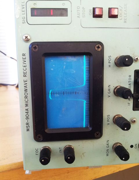
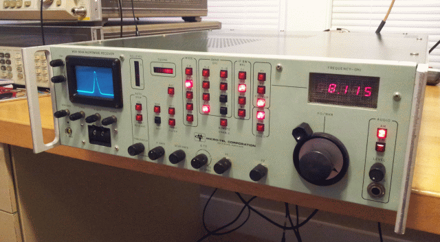
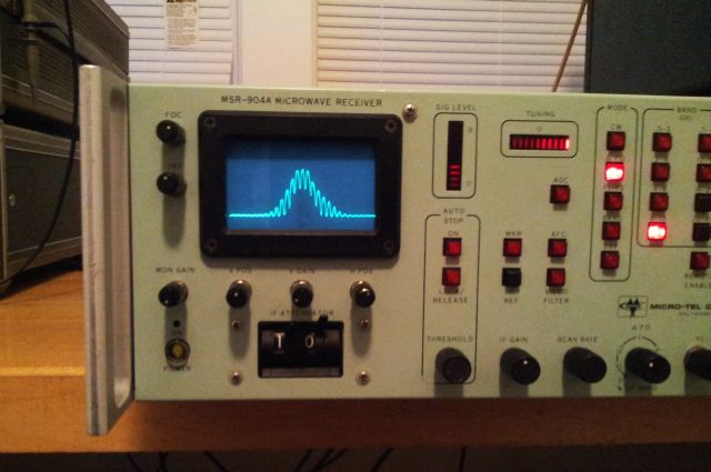
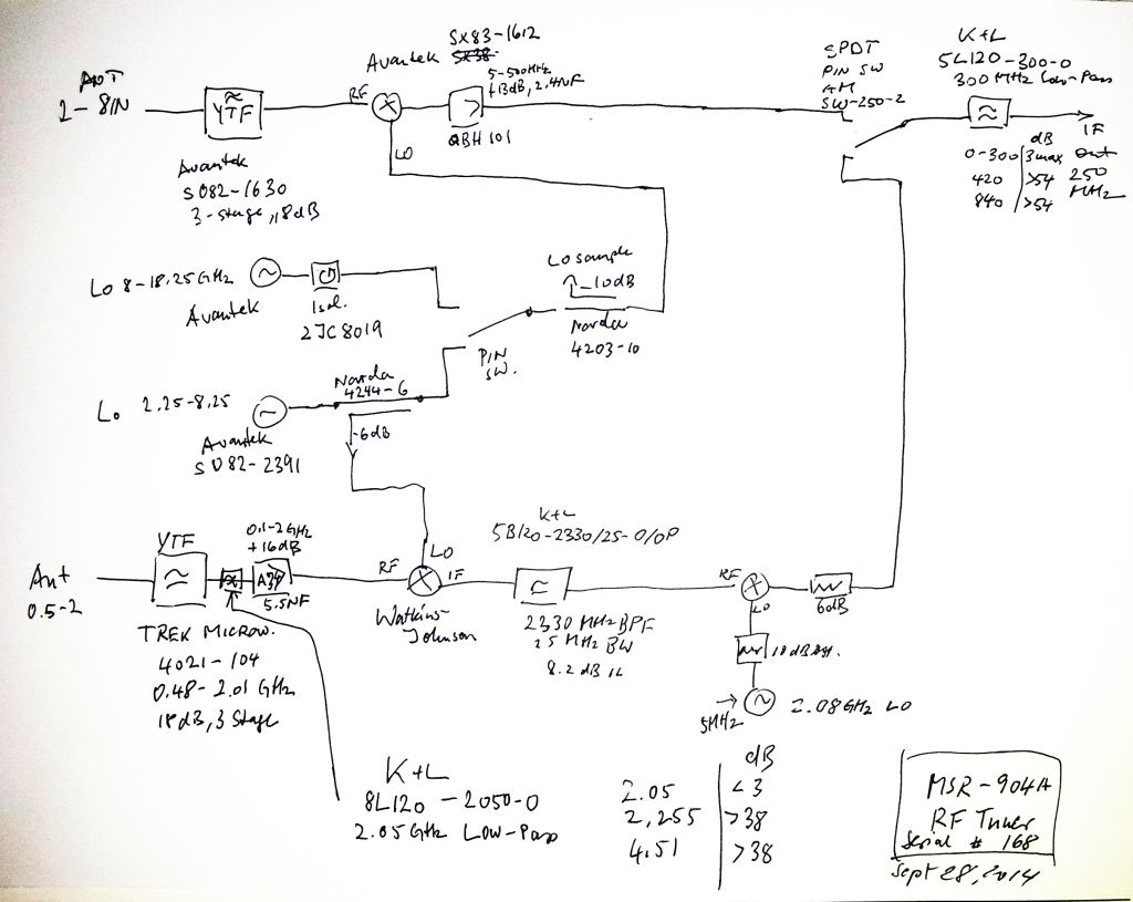
The current circuit, which is intended to be a reference signal conditioner for a Micro-Tel MSR-904A Microwave Receiver, also needs a 5 MHz output – the PLL will run off 10 MHz, but the MSR-904A still is ancient enough to require 5 MHz (5 MHz used to be the standard reference frequency from early times up until the end of the 70s – since then, 10 MHz is almost exclusively used, and sometimes, 100 MHz, for double-digit GHz circuits).
Such 5 MHz output is easily realized by a divider circuit, based on a 74F74.

Now, how do we achieve all this. Well, here is the schematic:
ref signal conditioner schematic

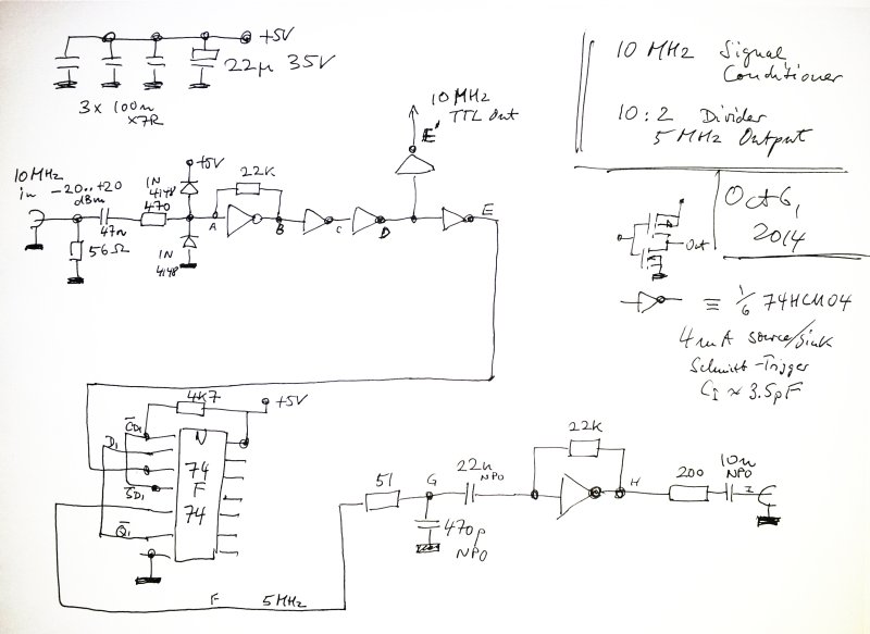
The essential part – a 74HCU04. This little circuit is extremely useful – get a handful of these, they are not just “inverters” but acutally work at frequencies from DC to many MHz, can source and sink at least 4 mA to 5 V. The 74HCU04 is more or less a set of 6 push-pull MOSFET pairs, in a handy package. These pairs can also be paralleled with no precautions to get more current, if needed.

The signal input is protected by a 56 Ohm termination (which can burn out if you feed excess DC or more than 0.25 W of RF – unlikely to happen). Then, there is a 47 n decoupling capacitor, a series resistor, and a clipping circuit – which will most likely never be activated.
The 22k resistor, along with the first inverter, and the 470 Ohm resistor form the first amplifier.

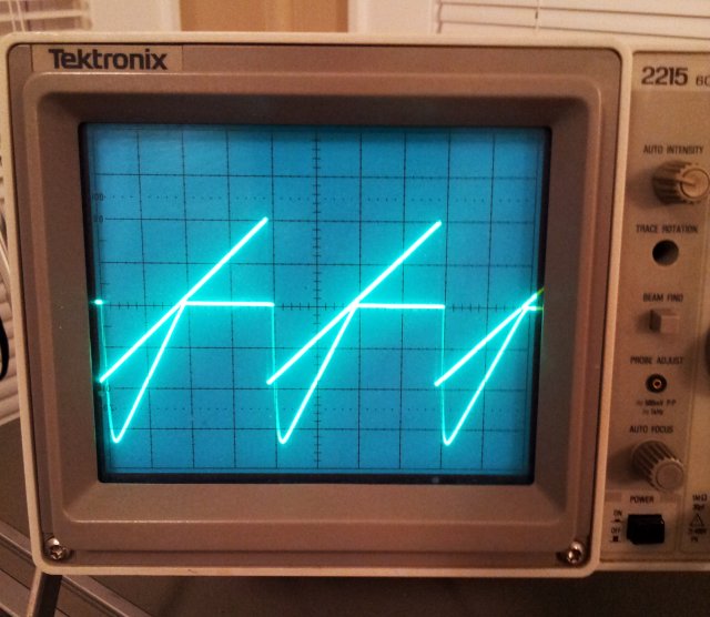
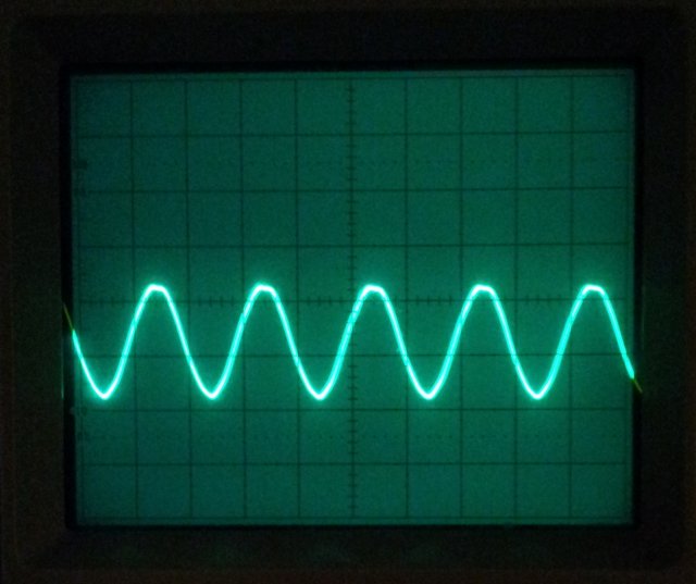
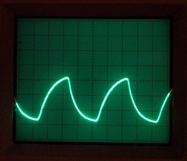
Signal A (see letter on schematic, input of first inverter):
ref signal circuit A
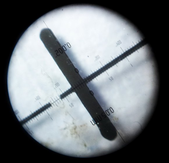
-scope is set to 1 V per div vertical, 50 ns per div horizontal.
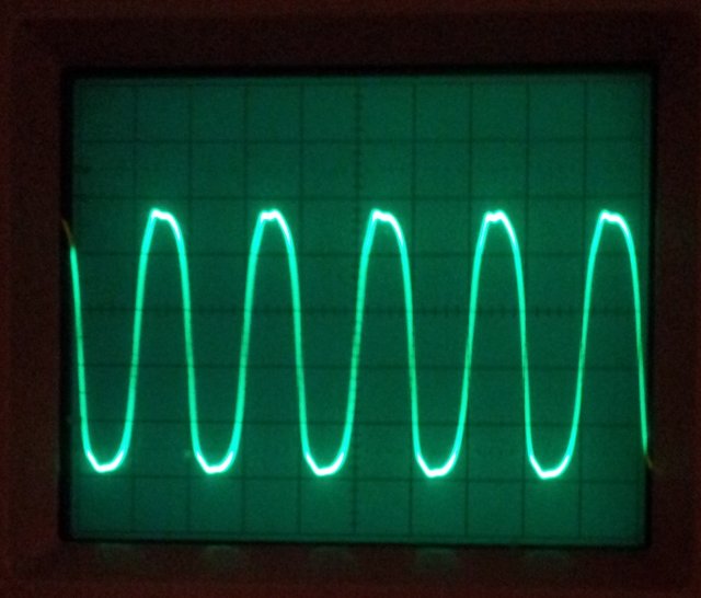
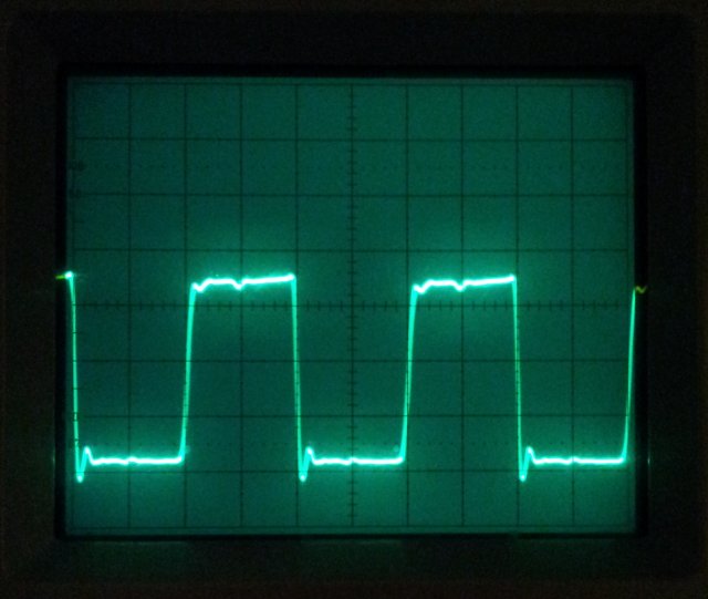
Output B:
ref signal circuit B

Note that the first gate is self-biased, no need to adjust anything.

This is then squared-up by the limiting action of the following 2 inverters:
ref signal circuit C

ref signal circuit 10 mhz E 1 v-div 50 ns-div

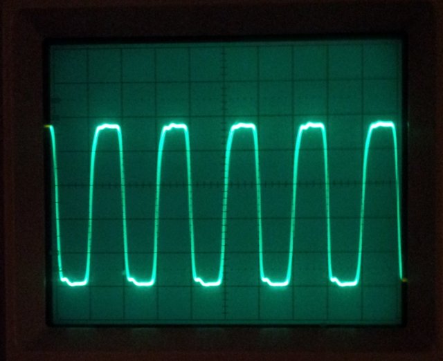
Now, we have a clean 10 MHz square wave. This is fed to a 74F74 edge-triggered flip-flop. The 74F74 is pretty fast, it easily works up to 100 MHz and will provide fast-rising edges.
The flip-flop will also ensure pretty much exact 50% duty cycle of the 5 MHz output.

ref signal circuit 5 MHz F

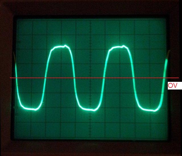
The output is fed through a low pass, 51 Ohm – 470 p, about 6.6 MHz, because we want low jitter at the divider stage (fast rise time pulses feeding the flip-flop), but not too steep edges at the output:
ref signal circuit G

After amplification by another 74HCU04 inverter:
ref signal circuit 5 MHz H
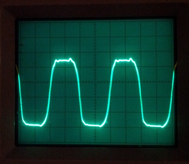
– this signal is still referenced to ground, and after another resistor and capacitor, finally, an AC signal, that can be used for various purposes, including frequency locking a MSR-904A.
ref signal circuit 5 mhz output I

Note: when you measure in such circuits, always use a >10 Meg, 10:1 low capacitance probe. Otherwise, you will get results, but these won’t reflect reality.

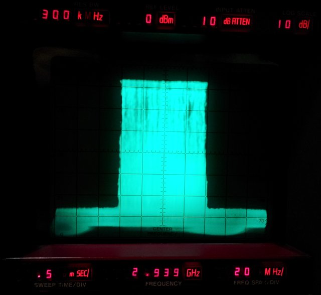
A quick test with a 10 MHz test signal – the circuit works well from about -22 dBm to 20 dBm, no issues at all. For the specification, and to ensure that is is working even under awkward conditions, we might limit it to -10 dBm to +16 dBm.

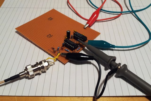
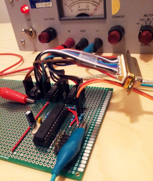
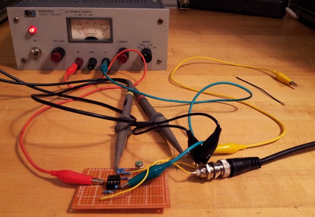
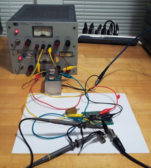
The little thing in action:
ref signal circuit test setup

Micro-Tel MSR-904A Microwave Receiver: remote control (digital interface)

The MSR-904A has a remote control interface, to control most of the front panel settings by TTL level signals – operation mode, band, filters, IF attenuator, detector. All in all, 22 signal lines are needed.
The circuit will also need provisions for latter addition of the PLL filter and PLL control – just a few digital lines. All will be controlled by a single USB interface.

First, we need a cable – the MSR-904A uses a DSUB-37 connector, but not all pins are used – so an adapter cable was fabricated to convert this to a much more common (and available) DSUB-25:
msr-904a remote control cable
– quite a few wires!

msr-904a remote interface wiring and register layout

The digital control is implemented by a set of three 74LS164 shift registers, serial in, 8 bit out. These registers are very fast, can be set in a few microseconds. The three registers are named 1-Q0 (LSB of register 1) to 3-Q7 (MSB of register 3).
The micro is an ATmega8-16PU, running at 16 MHz – this has plenty of power to handle the USB interface, the digital control, and later, the PLL loop. There is also a standard 10 pin ISP header, not shown in the schematic.

msr-904a digital interface schematic

The circuit – build on a perfboard. No plans to fabricate a PCB, I don’t anticipate a big demand for MSR-904A remote control units, but still it should last many years. This is why a proper FR4 perfboard with plated-through holes is used.

msr-904a digital interface

HP Fundamental/Harmonic Mixer 5086-7285 (22 GHz): digital bias control

In an effort to build a 2-18 GHz down converter, a HP mixer 5086-7285 needs to be controlled. This is one of a group of 22 GHz mixers, all used in earlier HP spectrum analyzers. These mixers are very linear, and useful both at fundamental and harmonic frequencies.

That’s the little magic thing, and the frequency list-harmonics:
5086-7285 mixer
5086-7285 mixer harmonics

All in all, at a first glance, pretty easy to use – it only needs +10 and -10 V power supply and bias for the diode.

Well, bias, after looking through the schematics, this is the assembly taking care of it: a board full of resistors and amplifiers, with no less than 22 (!) adjustment pots.
08565-60023 bias assembly

The interesting part are the bias drivers itself –
hp bias circuit for harmonic mixer
– the linearization, etc., this can all be done easily by using digital memory and a DAC nowadays, but the drivers, we still need them.

The bands B3 and B5, the even harmonics, the things are clear and as expected – a voltage source, and a resistor. Easy enough. But, what did HP do for the odd harmonics?? – the are a few extra resistors around the opamps, and these resistors make it a tricky thing. Too tricky to make it easy to understand. Some kind of negative resistance circuit/kind of a voltage to current converter, which depends a bit on the load resistance.

So, what do you do to understand such things better – build a little test circuit, here we go:
mixer bias test circuit
-it is essentially the same circuit, as for the B1/B4/B2 bands, U6B of the HP circuit- just left out the switching transistor.

It works pretty well, and as a U to I converter, see here:
bias driver test 200 mv-div ramp  1 mA-div current
– ramp voltage is the drive signal, 800 mV p-p, 200 mV per div (center line is zero). During the negative signal period, the output is active – current signal is 1 mA per div (center line is zero).

Having the basic functionality of the ciruit confirmed – some calculations with LTSpice, one of the best general purpose analog simulators around, Thank You, Linear Technology!

Here the files, in case you want to investigate it yourself:
hp mixer bias

This is a typical result, mixer bias current, vs. input voltage of the circuit, at resistance (of the mixer), of 950 (steepest)-1050-1150-1250 ohms.
r6-92 1-9 bias rscan vs Vi
So, this cirucit really is a U to I converter, with the slope depending on the load resistance.
Also note the model circuit of the mixer internal resistor and diodes. The two diodes and the 970 Ohm resistor are the result of bias current vs. bias voltage measurement. Bias voltage is in the range of -1 to -7 volts, about 0 to 8 mA.

With these findings, next step will be to build a driver circuit that can work fully digitally controlled, with no adjustment pot at all (series resistors will be manually selected).

YTO YTF Driver: 0..250 mA, 16 bits resolution

Quick update on the YTO/YTF driver board – with 16 bits of resolution. Assembly, is complete, and basic function has been checked – digital control test will follow tomorrow.
Current is settable from 0 to 250 mA, with 65535 counts of resolution – about 3.8 Microamps per LSB. All has been build to minimize noise, with heavy filtering on the supplies. The DAC is run from a dedicated 5 V supply, with a 2.5 V precision reference, 1 ppm/K, MAX6325ESA+.
The U to I converter is powered by 11.4 V – provided by a LM317 voltage regulator.
Switching element is an IRF730, operated as a series variable resistance in series with the coil.

YTO YTF driver 2x250 mA 16 bit

YTO YTF driver 2x250 mA 16 bit schematic

Looking at the BoM, the parts sum up to about USD 35 plus board, not bad – target is to stay below about $100 for the final assembled unit, which will be achievable, no issue. Main cost comes from the MAX reference, and the DACs (DAC8830), almost USD 22.

To come: bandwidth testing

YIG tuned oscillator (YTO) / YIG tuned filter (YTF) driver: digitally controlled current source

For a digitally controlled YIG oscillator and filter, a driver is needed that can convert serial data from a microcontroller to a well defined, stable, and low noise current.
Bandwidth of the circuit should be a few 100 Hz, and maximum current in the 300 mA range, so it needs to run of a reasonably high supply voltage, otherwise, the inductance of the coil will limit the slew rate. The YTO needs about 120 mA full scale, the YTF about 260 mA.

I might do some fine tuning on the DACs later or change the current sense resistors for a 2.5 V drop at close to max current, for best signal to noise ratio, but for the test circuit, 10 Ohm RH-25 resistors will be used. The current sense resistors are a very critical part – they need to be low drift, over time, and over temperature, regular resistors, with 100 ppm/K or more will only cause drifting frequencies, and trouble.

Here, the draft schematic, as-build:
YIG driver schematic dac control - u to i converter

That’s the test setup, with +20 V and -10 V power supply, for the YIG. In the final setup, there will be independent, filtered and regulated supplies for low phase noise.

YTO driver test setup

The circuit is driven by a HP 8904A signal generator, with independent adjustment of offset and voltage. Here, the output at 70 mA current, with a +-1 mA amplitude variation:

YTO output 70 mA +-1 mA
YTO is a HP 5086-7259, 2.0-4.5 GHz (nominal).

So, about +-40 MHz – close to expected +-35 MHz.

Bandwidth analysis will follow.

Here a quick calculation of the DAC resolution, 1 LSB will be about 0.13 MHz, more than sufficient for the DAC tune. The DAC used, a DAC8830ICD has typical +-0.5 LSB non-linearity, max +-1 LSB. Additional tuning will be easily accomplished by the FM coil, using a PLL.

yto ytf dac calculator

Micro-Tel MSR-904A Microwave Receiver: a broken trace, a replaced pot, and an escape proof guarantee

First of all, mystery solved – the remote enable input for the IF attenuator. After quite painful tracing of wires and disassembly of the logic boards, a broken trace! Just a little crack, but big enough to block the electrons’ flow. A little bit of solder, and then, suddenly, the MSR-904A’s IF attenuator can be remotely controlled.

Today, a also the dual pot for the F2 adjustment arrived – fitted, also this, working again.

But most interesting, a little box, with a label not seen before:

msr-904a mains cable label

The part has a NSN number, original unit price was no less then 71.38 USD!

Enclosed – the most special mains power cable I have ever seen:

msr-904a mains cable
-it was well packaged in a multilayer heat-sealed bag.

And, a label, which will be kept – Federal Prison Industries: Escape Proof Guarantee
unicor federal prison industries escape proof guarantee

Micro-Tel MSR-904A Microwave Receiver: crosshair, imagesetting film printing, remote control input

Some more progress related to the MSR-904A:

(1) The crosshair. The old one is badly damaged.
msr-904a crosshair

Sure, I could just use a laser or inkjet printer, but with a laser, the resolution is not good-doesn’t look sharp enough. With inkjet, I doubt it would be permanent enough, and also there, the printout is never sharp enough. So I decided to go for the solution that also Micro-Tel used, so-called imagesetting film. Back home in Germany, not problem, but here – first I need to find a source. Turns out, not too difficult, about 20 USD for 8 pcs of crosshair (minimum order fee), a company located in New Jersey, not around the corner, but not far. 2400×2400 dpi, acetate/emulsion film.

With a film printing service identified, we need to get the digital data, of the crosshair. With the human eye being a pretty precise tool to determine even small differences, and aiming for perfection with the replica – first, determined the line width and distances with a measurement microscope. Such a little microscope is extremely handy, I use it all the time for inspecting circuit boards, etc.

msr-904a crosshair measurement microscope

msr-904a crosshair measurement
one of the big divisions: 0.275 mm (26 pt at 2400 dpi) wide. Line is about 0.125 (12 pt at 2400 dpi) wide.

Here – a reconstruction drawing:
msr_crosshair

The new prints should be in the mail tomorrow!

(2) The remote control input: a 37 pin connector! Fortunately, not all wires are connected (x in the draft).

msr-904a remote control input

Controlling the function, bands and IF bandwidth, and detector characteristics (log-lin), all fairly straightforward. All of these inputs seem to have pull-up resistors, so grounding them works fine to switch. This is quite hand for control via optocoupler – no external voltage required.

The IF attenuator – traced the lines to the control board, it is a BCD control input, 2×4 bit. Unfortunately, I can’t get it to switch… the ‘enable’ signal doesn’t seem to reach the control board – more effort will be required to trace this last line! – Solved: a broken trace on one of the logic boards!

Some of the pins, despite having wires attached to them, remain unidentified – or might be reserved for options not implemented. Except for the IF attenuator control enable signal, all functions needed have been identified anyway.

msr-904a remote control input pinout

(3) The remote frequency control input – analog voltage: quick check with a frequency counter connected to the LO sample, and a DC voltage supplied – it is a 0 to 10 V input.
Scaling of the input voltage can be adjusted on the A6B2 board, R56 is for the mid-range adjustement (offset – supply 5 V and adjust for mid-band frequency), R68 is the gain adjustment (set at 0 V, and adjust for lower band limit; check setting at 10 V – should be at the high end of the band – and it really is).

Micro-Tel MSR-904A Microwave Receiver: some progress

With the basics done (power supply, potentiometer), a few hours were spent to get everything tuned up.
And, quite amazingly, it is receiving:

msr-904a first sign of activity
– notice the dirt, and the sticker residues. Also the crosshair (which is printed on a piece of plastic foil), will be replaced.

Finally, the exterior. The front panel, easy enough, all brushed and cleaned with diluted isopropyl alcohol.

The top, bottom and side panels with the sticky green stuff – all the old junk (“paint”) has been removed, my soakin the panels in methylated sprits, sanding, solvent cleaning, sanding. Then, a layer of aluminum primer (self-etching automotive primer). Followed by a light sanding, and a layer of ‘Hunters Green” alkyd paint. After 10 hours of air drying, final curing at about 150-170 deg C, for a bit over an hour.

All in all, quite an effort. The result –
msr-904a panels - newly painted

Missing items – one fastener like this – no idea where to find, seems like a part from the aerospace industry.
micro-tel quick release fasteners
Should you have any of these around, even of somewhat different length, or if you know a source, please let me know!

msr-904a receiving at 8.1 ghz
Sweeping test around 8.1 GHz – with the refurbished panels installed.

Two more handles are still needed – either need to get spare handles from a parts units (which may be impossible to find), or ship the MSR-904A with 2 handles only, and provide the remaining two later, once I had a chance to fabricate them back home in Germany. At least, I have the exact dimensions measured, just a matter of some CNC milling.

msr-904a receiving AM modulated signal at 8.1 ghz
-this is a test using a 8.1 GHz AM modulated signal, with about 1 kHz modulation frequency. Carefully checked the IF chain (different chains are used, depending on filter setting) – the MSR-904A uses 250 MHz, 160 MHz (by mixing the 250 MHz IF with 410 MHz, from a low noise LO), and 21.4 MHz (for the 100 kHz BW setting).
All seems to be functional.

With the receiver now basically functioning – some weekness of the AFC circuit alignment, and the frequency control was noticed. Therefore, some more effort was spent on the frequency control and AFC circuits, and the tuning indicator circuits. Really tough without any instructions or schematic.
There are some nice indicators on the front panel, LED bar graph displays – one for signal strength, and one for tuning.

These displays, now, in working condition and properly adjusted, are great fun to use. They are extremely responsive – nothing to compare with the time lag and sluggish nature of a modern SDR.

After several hours – here, receiving at 6.1 GHz, with 1 MHz bandwidth, and the AFC keeping the frequency, counteracting artificial drift:
msr-904a receiving at 6.15 GHz with AFC active

Monitoring of the AFC control is by looking at the IF frequency, 250 MHz (on the EIP 545A counter), derived from the (non-phaselocked) MSR-904A LO frequency, minus the RF input frequency (from the Gigatronics 605 Microwave Synthesizer; the EIP 545A is locked to the 10 MHz signal from the 605).
This setup allows me to check for any drift of the MSR-904A IF chain (and AFC, if activated), to 1 Hz resolution.
Had it running now for several hours, no issue, signal stays perfectly tuned.

The only remaining item, internally, is the alignment of the cross-band assembly – still lacking one CD4051 multiplexer circuit – which is on its way. A quick check with a CD4051 taken from another board showed that there is no defect, the board just needs some alignment of the band-to-band transition points. The crossband assembly allows a full 0.5-18 GHz sweep, with automatic band selection.

Micro-Tel MSR-904A Microwave Receiver: the monitor output

The MSR-904A has a few outputs (and inputs), most of them, easy to identify, but two, are pretty much a mystery to me, with no schematic – their function is clear, but with all these wires TTL logic boards -difficult to guess the pinout.

msr-904a monitor output

The more easy thing first, the monitor output. Arguably, this was intended to be connected to storage displays, digitizer, chart recorders, or the like – to more permanently record the activity over the bands.

So, what do we have. Using a scope, and a multimeter, and activating more or less all the functions of the apparatus, that’s what I found out.

msr-904a monitor output - pinout

Sorry for the rough draft, but any questions, please ask – for the given purpose, good enough.

The only pin that doesn’t do much, is pin 9 – always stays on logic 5 V – maybe a +5 V supply line? Doesn’t seem to be an essential function, anyway.

Micro-Tel MSR-904A: RF tuner block diagram and component specs

Just to learn a bit about the way Micro-Tel was doing their engineering, let’s have a quick look at the way in which it functions, at least for the RF front end. After some study and tracing, here is the block diagram:

msr-904a rf tuner block diagram
Some parts don’t have model numbers – because these are hidden, and I don’t want to take the thing apart.

Luckily quite a few of the parts are still available, and datasheets are available for most. The YIGs are Avantek, have a customer part number, but I assume, essentially, slightly modified line item parts, with some specific specications. The only really uncommon part, is a “TREK MICROWAVE” 0.48-2.01 GHz 3-stage YTF. Didn’t know that such low frequency YIG filters existed, this has serial #00003.

YIG filter 4021-104

Even more, TREK doesn’t ring a bell for me, and the filter really looks very much like Systron Donner technology, with the characteristic color, and square-cube shape.

As it turns out, TREK acquired the YIG division of Systron, some time around 1984… so, this mystery solved.

The only part where no data seems available is the 2-18 GHz mixer, Avantek SX83 series, but can’t find a -1612 model anywhere.

Some datasheets:
5B120-2330_25-O_OP – 5915011438953 _ chebyschev 2330 MHz 25 MHz bw

k&l 5L120-300-0 low pass 300 mhz

8L120-2050-0 low pass – 5915012428744 _K&L filter

narda 4244-6 082-Couplers

a34 datasheet

qbh 101 amplifier datasheet

narda 4203-10 coupler