All posts by Simon

Harrison HP 6202B Power Supply

A quick repair job – an old but trustworthy Harrison (HP) 6202B powder supply. 0-40 Volts, 0-0.75 A.
This is quite a useful range, has overrange to about 45 V, and a good compagnion for a 6200B supply that I have been owning for a long time.

This is it:
harrison 6202B

A suspicious label:
6202B label

It worked well, but had excess noise and some oscillation, when loaded. BTW – no fancy dummy load here:
dummy load

The inner workings –
620BB circuit

After some clearing, more or less washing it with isopropyl alcohol, I found this capacitor, date code 6708 – February, 1967, not quite 50 years.
6202B defective capacitor

After a few hours of test run, under about 50% load, a quick check – at various loads, with and with out current limitation. That’s the kind of noise I’m getting. It is mainly 60 Hz ripple, about 2-2.5 mV p-p; maybe 1 mVrms – a bit more than the 0.2 mVrms specified by Harrison – but still in the same range as the Vrms noise of modern power supplies.
6202B noise

Ultralinear ADC – some mathematical review

Working a bit deeper in the topic of ADC calibration, and doing some math some preliminary conclusions reached so far:

(1) Analyzing the ADC noise, requirements to suppress mains noise, and the effective number of bits available from the ADS1211, I figure that running the ADC at 60 Hz data rate would be the best choice (50 Hz in Europe, will be factory-settable in the final apparatus), and a data volume that can be managed easily. To get the best ENOB per reading, the ADS1211 is run in 16x turbo mode, 2083 decimation, 4 MHz clock (will be 16 MHz:2 later, running on one clock with the controller, just lacking a 8 or 10 MHz crystal atm).
59.98 Hz resulting frequency, close enough. For 50 Hz, we will run at 2499 decimation, and get exactly 50 Hz data rate.
With a 4 MHz clock, about 22 bits effective resolution, with 10 MHz, even 23. Not bad, but I’m sure the test setup will be a bit worse (better reference, shielding, improved power supply needed, for the analog supply -low noise, will be based on LM723 – which is actually still a very well performing circuit, and much lower noise than the common 78xx regulators).

(2) Calibrating an ADC, to, say, 21 bit effective resolution, which two million noise-free counts, 128 dB SNR, with a sine wave by generating a histogram: it will take a long time. A very long time. 60 Hz means 5 million samples a day, would need to collect readings for several day – doesn’t seem practical.

Next steps:

(1) Noise characterization, shorted, and with a somewhat noise signal – this will tell us a bit about the nature of the local non-linarities, by comparing the noise histogram, with Gaussian noise. Will also show missing codes, if any.

(2) Do an in-depth characterization of linearity for one exemplary ADS1211, might need above-mentioned improments to reduce noise effects in the test setup, and also needs low jitter clock source (current crystal should be low jitter, but might want to change to 8 MHz before going to a lot of trouble with characterization. Key question is, for the ppm-level linearity – is this locally worse at certain codes-in certain small code regions, or evenly spread over all codes, just needing a few “pin points” for a correction algorithm, to get the linearity down to 1-2 ppm level.
After review of the literature, a method of fitting sine-wave data (similar to histogram method, but rather than just counting the bins, fitting the data – voltage vs time – to an ideal sine wave, with a 4 parameter fit, and using the residuals for non-linearity estimation; fit might be done piece-wise, for big datasets, to allow for some small frequency drift of the sine source; might also cut-off the uppermost and lowermost bins, minimum and maximum voltages).

(3) Decide, based on the data of item (2) how many measurements/level will need to be measured to continuously monitor the performance and adjust correction constant. In the final system, a 16-bit ultrahigh precision DAC/programmable voltage source. Such kind of circuit can be build from discrete low-drift low-tempco resistors like Alpha Electronics MA series, and a precision low noise/low drift reference like the LTZ1000 or LM399, and a few opams, like LTC1051.
It would be fairly easy to sample these 16 voltags with the proposed 4-ADC scheme, and calculate corrections coefficients, at the 16 points, to compensate the the major part of the non-linearity.

Probability density function – calibrating the ADC: test run with the ADS1211

To further advance the ultra-linear ADC project, a little test setup has been deviced. Naturally, the final setup will require strict low noise construction, with only the best low-drift parts in the analog chain, and so on. At the moment, I just need to get to code running and tested to some kind of precision, therefore, a makeshift assembly will be good enough.

For the ADC, an Texas Instruments ADS1211 24-bit sigma-delta ADC, with a 4-channel MUX has been selected, simply because I have it around, and it has a good accuaracy to start with, about 15 ppm non-linearity, and no missing codes up to 22 bits.

A diagram from the datasheet, the non-linearity looks fairly well behaved – my confidence in hitting the 1 ppm mark is growing!
nonlinearity ADS1211

The ADS1211 is really a great part, for what it is, and for the price (about USD 25 each), and I have been using it a for a major projects in the past, 3 or 4 years ago.

The build in 2.5 V reference is not the most stable and quiet, but will do for now.
Input is configured for +-10 V bipolar, using 3.9 k-1 k Ubias resistors.
Clock frequency is 4 MHz, a sub-harmonic of the 16 MHz of the ATmega32L controlling it (again, the famouse JY-MCU board).

ads1211 test board

A simple trick for soldering SOIC parts to a 0.1″ pitch prototype board: just place the part on the table, upside down, and bend down, with a screwdriver, every second pin. It will be working just great, and no issue at all with soldering it, even if you don’t have good tools at hand.
No need at all for any special SMD boards, etc., just a waste of time, from my point of view.

Now, for a quick test, connected a sinewave (10 Hz), and sampled at a few Hz.
More cables than actual parts.
ads1211 atmega32l usb interface

With the sinewave at the input, and constantly sampled, the ADC output should resemble the sine function – however, we don’t want to analyze each measurement individually, but will collect massive amounts of data, and put them into bins – looking at the sine function, not all output values have the same probability – the values at the extremes will be more frequent, because there, the sine function is more flat than close to zero. No need to give the exact maths here, just a little diagram:
sine pdf diagram

In the final application, we will cut-off the outer parts, and just use the middle section. For today, that’s the result of a quick test:
ads1211 sine signal histogram result
Well, quite satisfactory for a start – next step will be to figure out the details (sampling rates, data transfer protocols to avoid lost samples, fast code to sort large number of samples; also, need to find out how the local varation of nonlinearity related to the larger-scale variation – by sampling for several hours…). Will all be done, step by step.
Another idea is to measure the frequency/period of the sine test signal, and using the zero-crossing as a sync pulse, to time-stamp/calculate the acutal voltage at a given time, and correlate by a least-square of similar algorithm with the ADC digital output.

Low distortion sine generator: the source of very pure waves, digitally tunable

For the ultra-linear ADC endeavour: Generating low distortion sine waves is actually, down to about -80 dB, not really a challenge. Wien-bridge oscillators will to the job. There is a related, very popular scheme – the state variable oscillator, chiefly, SVO. It is more or less just a chain of 2 integrators, an adder, and some regulation circuitry, to keep the gain at exactly 1 and the amplitude stable. It will deliver 2 signals, at 90 degrees phase shift.

For general instruction, just have a look at the schematics of the Tektronix SG5010 Low Distortion Audio Oscillator, or the marvelous HPAKeysight 8903A Distortion Analyzer. There is also a very comprehensive article in one of the HP Journals, just have a look around the web, plenty of details out there.

For the design, I selected a UAF42AP for the integrator opamps, because this part is quite handy, and an MPY634KP analog multiplier to get the gain stable. The signal level is sensed with a simple opamp rectifier, and a damped low-pass is used for the gain stabilizer (leveler). The gain stabilizer by rectification, I just put it in as a temporary fix, lacking some analog switches (DG201) that will be used in a sample-and-hold circuit.
Also the UAF42 will be replaced later, most likely with some LME49710, which are currently resting back in Germany.

The integrator time constant of both integrator are controlled by 2 multiplying 12 bit DACs, AD7543JN. This will allow (1) tunable frequency, and (2) reduction of harmonic distortion by adjusting the tracking of the two integrators, with some inevitable differences of capacitor values, and so on. The frequency tracking will be step-wise, no change of any settings during the ADC sampling period.

A little draft (let me know if you need help reading – proper schematic to come, once design is more mature), just to help you understand:
state variable low distortion oscillator draft
You can see the integrators, the resistive network of the multiplying DAC, and the output. Leveler and multiplier not shown. Both signals (0 and 90 degrees) are fed to the leveler circuit, to reduce ripple a bit. Very long time constants are needed, to avoid impact of ripple on distortion – will need to analyze, and replace with a better leveler circuit (digitally controlled sample and hold, on both the 0 and 90 degree signals). The leveler circuit will also generate useful SYNC signals for the ADCs – most likely, I will link the sampling to a multiple of the calibration signal or use the SYNC signals to discard measurements over certain portions of the sine waveform.

That’s how far things have advanced. It’s running with +-15 Volts, and 5 V digital supply, and controlled by an ATmega32L via USB. Later, I might keep the ATmega, and use this as a slave controller, via a serial bus.
state variable low distortion oscillator MPY634KP UAF42AP AD7543JN

Measurements to come. Stay tuned.

High resolution ADC implementation: linearity, almost perfect

At first glance, it is a straightforward request: measuring two voltages representing the cartesian corrdinates of a point, lets call the voltages Ux and Uy, and calculating the polar representation of it, the square root of the sum of squares. In fact, the later part is already irrelevant for the current topic, the only important fact is that this calculation needs to be done in a way that if Ux=13.000000 and Uy=5.000000, resulting in R=sqrt(12^2+5^2)=13.000000, is fully symmetrical for Ux and Uy, i.e., the same result must result if Ux=5.000000 and Uy=13.000000.

This can only be achieved if for both ADCs, the quantizer transfer function is perfectly identical. Simply speaking, for every voltage level applied, the resulting digital code needs to be the same, for both of the ADCs, X and Y.

A simple solution would be to use the same ADC, for both channels. However, this will increase random noise, because the integration time is only half of the available signal time. And, it is not applicable in the given case, because Ux and Uy change slowly but perfectly unpredictably over time.

Therefore, there seems to be no other way than measuring both values simultaneously, over well defined and synchronized time intervals, and then doing whatever calculation is required.
After spending 2 hours calculating, I can say, we need about 1 ppm linearity to make this work as desired, better, adding in some noise and unpredictable drift and error sources, 0.2-0.5 ppm linearity.
Also, I realized that a bit of noise would be acceptable, as long as it is coherent, and as long as it is affecting both channels in the same way. So cables and layout will be routed for as much symmetry as possible, and thermally coupled as much as possible.

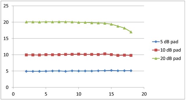
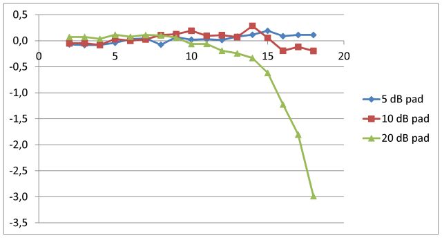
How can this be achieved? First attempt, even before I learned about this issue, was to use the best ADCs at hand, two Prema 5017 7.5 digit multimeters, but even these left something to be desired (4 ppm linearity deviation per channel, but seems to be a bit better than spec).
My first suggestion was to switch from the Prema intruments, to two HPAKeysight 3458A Digital Multimeters, these reach about 0.05-0.1 ppm linearity, in the 10 V range. Impressive, but 24 kg of instruments, worth about USD 20k. Not an option, except for proof of concept, which has been achieved using the Prema devices.

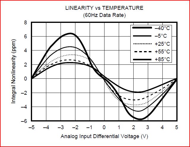
Now, what kind of intricate sampling scheme could be used to make this work, with off-the-shelf parts. Well, first we need a good starting point, a linear ADC. Looking through the various datasheets, let’s discuss a particular part, with impressive performance ratings, the AD7710. This is a 24 bit sigma-delta converter, and has +-15 ppm nonlinearity. So we need to find means to improve this by a factor of, say, 30 to 50. Seems to be viable, with some error correction meachanism. Also, we don’t want the error correction to cause any dead time of the system (i.e., there can’t be an autocalibration feature taking significant time, leaving gaps in the signal measurement).

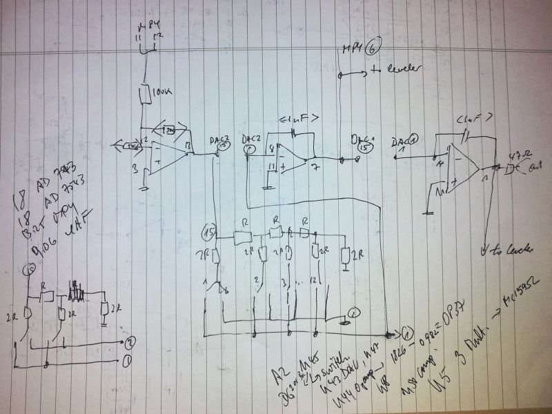
So, here is the proposed scheme:
ultra high linearity ADC sampling scheme

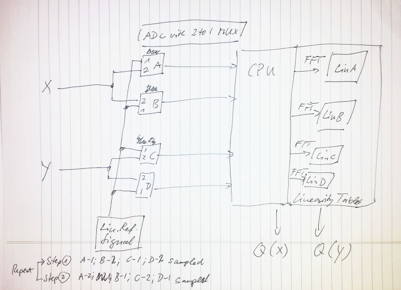
It’s a bit rough, buta acutally, not too complicated. What we intend to do is to use 4 ADCs (named A, B, C, D) rather than two, and to use ADCs that have a build-in 2 to 1 MUX, so it can either sample channel 1 or channel 2. The “1” channels, A-1, B-1, C-1 and D-1 are connected to a reference source that will allow analysis on ADC non-linearity, and the “2” channel, well, thats for the acutal X and Y signals.

The whole thing is connected to a CPU, which will require some kbytes of RAM and FFT/histogram processing powder, not an issue these days. It will acquire the digital representations Q'(X) and Q'(Y), and hold the non-linearity information for each of the ADCs (called “linearity tables”, LIN A trough LIN D) and use this data to calculate the corrected “ultra-linear” digital representations of the input voltages, Q(X), and Q(Y).

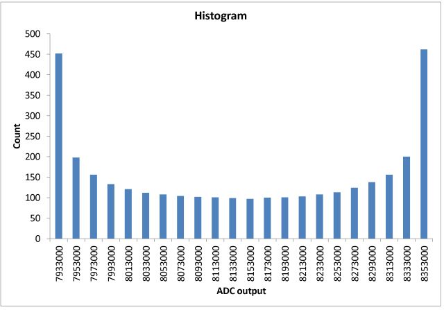
Don’t ask how I will calculate the non-linear correction coefficients. It’s filling piles of paper already, working through FFT and histrogram analysis, and might be some occupation for an upcoming rainy Saturday, to get this coded.

The sampling scheme will work with two steps: measuring a cal signal on A and C, and measuring X and Y on B and D; then, 2nd step, B and D cal signal, A and C – X and Y signal.

Next question, what is a suitable cal signal that can be samples to yield the non-linear properties. Well, as we are only interested in the relative non-linearities of the converters, there is more freedom to choose signals, e.g., a triangular signal, or a ramp function. But, as you might know, it’s not all that easy to generate a good linear ramp voltage – there capacitors involved, and opamp integrators, and we are talking low frequency here, lika a cal signal frequency of 10 Hz, and measurement periods of minutes, rather than seconds. This will make leakage current significant, and a lot of effort. And, we run the risk of introducing some second-order errors, so perferably, the correction scheme employed should acutally yield quantizer transfer functions of all ADCs that are as close to ideal linearity as possible.

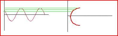
So, what signal to use. The solution is simple – we need a perfectly clean sine wave. This is predictable with time, easy to handle numerically, and, fairly easy to generate. For reasons of filtering, preferably, noise and distortion of the signal should be minimal. But, how much is minimal?
We will treat the signals, cal, X, Y, as a dynamic signals (slow, but steadily changing, with R, see above, having certain very low frequency components that we want to extract).

Some numbers: say, we want to resolve 2 volts to about 1 µV, that’s a resolution of about 2 million counts, in bits, 21 significant bits of information. This corresponds to a dynamic range of about 20*log10(2^21)=127 dB. Cross-check against the AD7710 datasheet shows that this is possible, for both dynamic and essentially-DC input conditions (with effective resolution of about 22 bits at 10 Hz sample rate). By averaging, to 2.5 Hz, we might win 1 bit, and get about 23 bits of useful information. That’s all falling into place; actually, it might even be better to sample at a faster rate, and do more digital averaging – this needs to be figured out later.

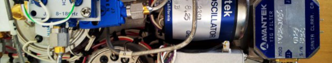
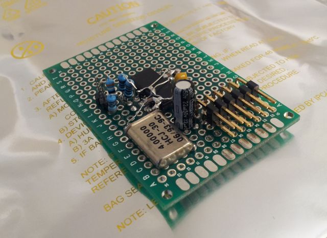
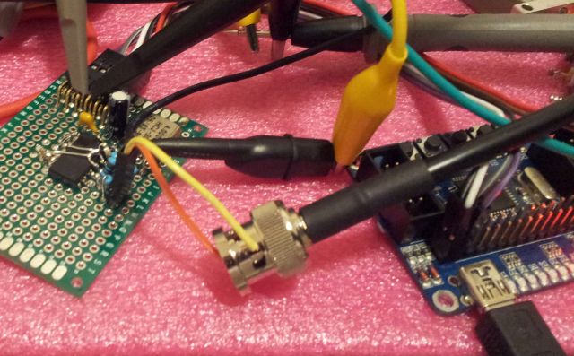
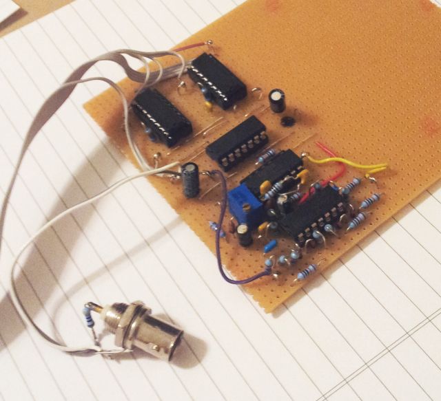
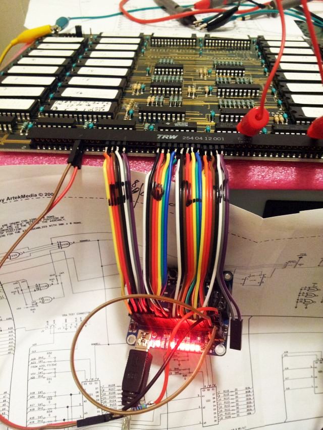
The ADC interfacing, at least the digital end, will be easy, just a few wires. The analog front end – also not too difficult, the AD7710 has a build in MUX, differential input, and the X and Y signals are available as low-impedance, very low noise signals. I might in fact put the 4 AD7710 in a little metal case, solder it all free-wire, and encapsulate it with a thermally conductive epoxy potting compound.

Next step will be to fabricate a low distortion cal source, of variable frequency. Frequency needs to be digitally settable, not too very accurate steps, but close enough, to keep it constant within drift and eventual changes of sampling rates/”integration times”.
Following above estimation, the distortion of this should be somewhere around -100 dB. It doesn’t need to be -130 dB, because some deviation of the transfer functions from ideal linearity will be acceptable in the given case – if anyone needs better linearity, just add a better signal source, keep the ADC setup thermostated -the limit will be only the stability of the non-linearity with time.
Well, -100 dB might be a bit tough to proof with the equipment I have around here, and with the relatively plain parts. Let’s see what is possible. And maybe build an improved version later.

HPAK 8763B switch test

The 8763B is a very useful device, a 4-port coaxial switch, and has been sold for many years by HP, Agilent, and still sold by Keysight today.
It is single-ended terminated, and has two latching switches.

8763b switch

Two of these will give a nice transfer switch, for auto-calibration (through-connection vs. DUT) of the attenuator test setup.

These switches are specified up to 18 GHz, and have a “max. 0.03 dB insertion loss repeatability”. Now, the big question is, what is the actual repeatability. Knowing the manufacturer, it can be 10 or 100 times better, but you never know. This is fairly critical, because a combined uncertainty of 0.06 dB, for the two 8763B forming the full transfer switch would be not acceptable for the purpose of calibrating attenuators to better than 0.1 dB precision/linearity.

So, quickly hooked this up to the not yet auto-calibrating setup, and recorded power traces, 40 points each, 1 measurement per second, and switching the 8763B in and out every 10 seconds (vertical lines).

This was done at 4, 8, 12, and 18 GHz, and for all ports of the switch.

The setup
8763b test setup
(green item on the right hand side is the feed line directional coupler, connected to the Micro-Tel SG-811 source; light blue test cable on the left is going to the Micro-Tel 1295 receiver).

The results (two examples; same finding at all frequencies) are not very difficult to interpret:

8763b test 1

8763b test 2

– There is not really any switching visible, and one can only judge that the repeatability is actually +-0.002 to +-0.004 – the noise of the measurement.

It seems the only way to get more accuarate data will be to measure the repeatability with the two switches in series, in the final setup. Even though I’m using high quality microwave test cables, 0.002 dB amplitude stability, at 18 GHz is a challenge.
Will need to let the source and receiver fully warm up and stabilize, and use long integration times, like several minutes per switching event, to get data of 0.001-0.002 dB resolution. For now, it seems the switches will add much less uncertainty to the setup as initally thought.

3562A repair: 32 kbyte of bad EPROM data….

Using the little AVRmega32L board, and the various plugs and cables, the two ROM boards (one good, one bad) were read, and all images of the ROMs compared. And, finally, the 6th EPROM of the lower byte – U106, only reads 0x00. That’s not how it is supposed to be. Also, after leaving the board switched on, U106 is warming up, much more than the others. So it is definitely at fault.

3562a U106 BAD EPROM

After some careful desoldering, the culprit was extracted. Cross checked the analysis with a regular EPROM programmer, and in fact, it is not working at all. Well, well. Now, just need to get a 27256 or 27c256, and this will fix the 3562A, and it can go back into service (imagine, this unit is still commercially used). Fair enough.

3562A Dynamic Signal Analyzer: reading the ROMs

I happen to have a 3562A for repair, which had a defective power supply, and after fixing this, it still doesn’t work – traced the error to the ROM board. It is really a coincidence that I own a more or less identical unit, which is working. Therefore, after checking all the supply rails to make sure nothing is going to damage it, I swapped out the ROM board with the working unit, and, there we go, it does the trick.

Now, how to find the defect? – first, a quick check of all the address logic, to no avail.

So the defect must be located in one of the ROMs. Have a look, the board has 2×18 pcs, Intel P27256, 32 kByte each:
3562a rom board 03562-66503 rev b

These chips are representing 589814 words of data (16 bit bus): a massive 1.179648 Megabytes, holding the program for the 3562a.

To get it powered up, first surprise, the thing draws nearly 2 Amps, about 55 mA each. Checked with the datasheet – and in fact that’s what these little heaters need.

Checking with the schematic, seems that this is an earlier version of the board, Revision B. That’s a pitty, because Rev C is much more common, and ROM images would be available off the web. Judging from the datecodes, manufactured in 1986. Still, a great instrument, low noise, build in source, and easy to use.

The circit of the board is really nothing special, a few decoders, and the memory bank, with some bus drivers.
03562-66503 address decoder

The plan is as follows:

(1) Read out the bad board (reading data from this first, just in case I accidentially damage something).
(2) Read the working board.
(3) Compare the EPROM images from both boards.
(4) Replace any defective EPROM(s). The ones installed are single time programmable, plastic case, but not an issue at all to replace them with regular UV-erasable EPROMs, if needed.

Desoldering all the 36 EPROMs – absolutely no option with the tools I have around here. With a few wires, and a ATmega32L board (JY-MCU AVR minium board V 1.4, always handy to have a few of them around), it was just a matter on an hour to get everything set up, not the fastest way, but the data will be clocked out byte by byte…

reading from the 3562a rom board 03562-66503 rev b

Now it is just a matter of time, for the defective chip to show up.

Attenuator calibration – first real dataset!

Some items of the mighty precision attenuator calibrator setup are still missing, like the automatic auto-zero/through calibration, and the adaption of the reflection bridge (see earlier post), but nevertheless, all parts are now in place to do some first real measurements (and generate, thanks to computer control, more data than anyone could have ever recorded manually, without getting close to nervous breakdown).

The device unter test (DUT). It is a HPAK 33321 SG step attenuator, 35 dB, in 5 dB steps – it is more or less a transmission line, with 3 resistor pads that can be individually switched in and out.
33321 sg step attenuator DUT

Also, note the SMA to SMA connector needed to get things connected vs. a through line. No allowance was made for this connector, it is a 18 GHz qualified precision part and will have very little loss.
hp 33321 sg data
As you can see, it is specified for 4 GHz operation – there are multiple models of these attenuators, both from Weinschel/Aeroflex and HP/Agilent/Keysight, up to 26.5 GHz or more. The 4 GHz models are relatively easily to come by, and others have claimed that these are actually quite usable up to higher frequencies. Let’s see.

While I don’t have exact specs for the 33321 SG model, there are similar models around, and typically, the numbers given by HP are +-0.2 dB at 10 dB, +-0.4 dB at 20, and +-0.5-0.7 in the 30-40 dB range. Repeatability about +-0.01 dB, which is quite impressive.

To be exact, we will be dealing with insertion loss here – not quite attenuation, but close, because no corrections have been made for any return losses (due to the SWR of the receiver and of the DUT, which might also change with attenuation setting).

Now, the test:

Step (1) – the system was calibrated without the DUT, just with the cables (from generator and to receiver) directly coupled (“through” calibration)
Step (2) – the attenuator was inserted, and tested at all the steps from 0 to 35 dB, 0 dB was measured twice. For all steps, 10 readings were taken, 1 per second, and averaged. Standard deviations are very small, showing the excellent short-term stability of the setup:
sdev vs frq at various attenuations

Step (3) – again, a through calibration. The measurements took about 3 hours – the drift was small, and distributed linearly with time over the measurements. Drift is pretty much independent of frequency. Later, there will be a drift correction anyway, by the yet-to-be-implemented auto-calibration feature.

Drift – 3 hours; about 0.1 dB absolute per hour.
drift in dB, 3 hours period

Insertion loss – at all the various steps, relative to “through” connection
insertion loss vs. through connection

Insertion loss – relative to “0 dB” setting. This is relevant for most of the practical cases, where the 0 dB values are stored in a calibration ROM, and the levels corrected accordingly. Repeatability of the 0 dB setting was also checked – standard deviation is about 0.04 dB, but might be much better short-term (more like the 0.01 dB claimed in the datasheet). However, keep in mind, 0.04 dB at 10-18 GHz is not more than a few mm of cable movement, or a little bit more or less torque on a connector.

insertion loss (corrected for 0 dB loss) vs frequency

Deviation of 0 dB corrected loss from the nominal values (5-10-15-20-25-30-35 dB steps)
total insertion loss - 35 db to 0 db, 5 db steps - deviation actual-nominal

As you can see, the attenuator works great well above the 4 GHz, easily to 12 GHz. Still usable up to 18, with some error. This error seems to mainly come from the 20 dB pad. Rather than relying on just the 20 dB pad measurement, some maths were done on the data to determine the insertion loss difference (attenuator switched in, vs. switched out), for each off the pads, e.g., for the 20 dB pad, by subtractions of these measurements:

(1) 20 dB in, 5 and 10 out; vs 0 dB
(2) 5 and 20 in, vs 5
(3) 10 and 20 in, vs 10

So there are actually 3 combinations for each pad that allow determiation of the actual insertion loss, for each individual pad. Furthermore, this utilizes the 1295 received at different ranges of the (bolometer) log amplifier, and with different IF attenuators inserted – and will average out any slight errors of the log amp, and calibration errors of the IF step attenuators of the 1295. For even more cancelation, the source power could be varied, but fair enough.

Results of a lot of (computerized) number crunching:

Insertion loss difference in vs. out, for each pad
attenuation of each pad vs frequency
The 5 and 10 dB pads are performing great, the 20 dB pad – a bit less. Well, there must be a way to tune this a bit – but don’t have a cleanroom here, and the fixtures, to scratch a bit of resistive mass from the pad, at certain places, etc. Wonder how they do this at the factory, and if in fact there is some manual tuning, at least for the higher frequency units.

Deviation from nominal, for each pad
calculated attenuation for each of the pads - actual minus nominal

This is really a quite striking level of accuracy – much better than specification, and also indicates the level of precision already achievable with the still temporary attenuation calibration setup. Up to 12 GHz, no issues at all.
33321 sg pad in vs out values

The 0 dB loss – some might be in the connectors, some in the transmission lines, some in the “through” switches of the 3 attenuators. Simply assuming that there aren’t any losses in the connectors and transmission lines, this is the loss per attenuator switch, when in “through”=”pad switched out” position.
0 dB insertion loss (calculated), per contact

All in all, the best way to use these attenuators obviously is to very accurately measure the 0 dB insertion loss, on a pretty narrowly spaced frequency scale. For the attenuator pads, these are best measured by recording values at various attenuations, and polynomial fits give very good approximation, without the need for a lot of density on the frequency scale, and seem to be merely additive, with little cross-correlation errors.
Sure, such things can all be analyzed with much more maths involved, but I doubt it will impact much the application-relevant aspects, and would be rather just a numerical exercise.

Micro-Tel 1295 receiver: parallel to serial converter – digital readout

The Micro-Tel 1295 has a GPIB (IEEE-488) interface, and in principle, can be fully controlled through this. In principle, but, not with ease; and, as it turns out, the build-in processor is running on 70s hardware, and doesn’t respond well to my National Instrument GPIB card. The only thing I need are the attenuation readings, in dB, same as shown on the front LED display.

Also, these GPIB cards are expensive, and I would rather like to control the whole attenuator calibration rig through one single USB port – also to be able to run in with various computers, not just with a dedicated machine.

In brief, after trying hard, I gave up – there need to be a more practical way to read the 1295 data.

First, how to get the data out, if not through the IEEE-488 interface? The case if fully closed, and drilling a hole, mounting a connector – NO. The modification should be reversible.
But there is a solution – the band selection connector, which is already used to remotely control the band switching, has a few spare pins!

This connector is a sight by itself:
micro-tel 1295 band control (and now serial output) plug amphenol wpi mini hex series 126

AMPHENOL/Wire-Pro “WPI” 9-pin “126 series” miniature hexagonal connector, 126-220; these connectors have been introduced in the 1940s, or latest, in the 50s. Still, available today… but the first piece of test equipment that I have ever seen that uses such kind of connectors. 500 Volts, 7.5 Amp – seems like a lot for such a small connector, at 14.99 USD each (plug only).

So, how to run the full display info over one or two wires? Update rate is 1 reading per second, or 1 reading every 4 seconds, not a lot of data – still it needs to be reliable, easy to use.
After some consideration, I decided to use a RS232 interface, with TTL level logic (rather than RS232 voltage levels-only using a short cable), and running it at 2400 bps, transmitting the data from the 1295 receiver to the main micro. This main controller, an ATmega32L can easily handle one more incoming signal, via its USART, and buffer any data coming from the 1295 before it is requested over the USB bus, by the PC software.

There are 5 full digits, plus a leading 1, a optional “+”, a leading-0 removing signal, and a blanking signal, which is set to low when the display is updating, or when the receiver is not giving a valid reading (over/underrange). Each digit needs 4 bits, binary coded decimal (BCD), so in total: 5×4+4=24 bits. Perfect match for the A, B, and C ports of a ATMega32L. This micro will monitor the blanking signal, and after sensing an updated display, read out the BCD information, convert it into a readable string, and send it out at the 2400 bps, via a single wire, no handshake, or anything. Will just keep on sending.

The easiest way to get the signal was determined to be directly at the display unit (A7) itself.
1295 a6 assembly schematic

There is also some space to fit the micro board, a commercial (Chinese, called “JY-MCU”, Version 1.4) ATMega32L minium board, with USB connection. These are really great, running at 16 MHz, with some little LEDs (which are on port B – disabled for this application), and a bootloader. It just saves a lot of time, and these boards are really cheap, below $10.

A 34 pin ribbon cable, with double row connector, salvaged from an old PC – so the controller/parallel-to-serial converter can be removed from the 1295 if no longer needed, and even the cable de-soldered.

The modified assembly
1295 a6 assembly top
MC14511 CMOS latches-BCD decoders-LED drivers – very common for 70s/early 80s vintage, and still working great!

1295 a6 assembly

Data is being transmitted, no doubt:
2400 bps signal

Now it is just a matter of some lines of code, and soon, some real insertion loss tests can start! Stay tuned.