HPAK 8763B switch test

The 8763B is a very useful device, a 4-port coaxial switch, and has been sold for many years by HP, Agilent, and still sold by Keysight today.
It is single-ended terminated, and has two latching switches.

8763b switch

Two of these will give a nice transfer switch, for auto-calibration (through-connection vs. DUT) of the attenuator test setup.

These switches are specified up to 18 GHz, and have a “max. 0.03 dB insertion loss repeatability”. Now, the big question is, what is the actual repeatability. Knowing the manufacturer, it can be 10 or 100 times better, but you never know. This is fairly critical, because a combined uncertainty of 0.06 dB, for the two 8763B forming the full transfer switch would be not acceptable for the purpose of calibrating attenuators to better than 0.1 dB precision/linearity.

So, quickly hooked this up to the not yet auto-calibrating setup, and recorded power traces, 40 points each, 1 measurement per second, and switching the 8763B in and out every 10 seconds (vertical lines).

This was done at 4, 8, 12, and 18 GHz, and for all ports of the switch.

The setup
8763b test setup
(green item on the right hand side is the feed line directional coupler, connected to the Micro-Tel SG-811 source; light blue test cable on the left is going to the Micro-Tel 1295 receiver).

The results (two examples; same finding at all frequencies) are not very difficult to interpret:

8763b test 1

8763b test 2

– There is not really any switching visible, and one can only judge that the repeatability is actually +-0.002 to +-0.004 – the noise of the measurement.

It seems the only way to get more accuarate data will be to measure the repeatability with the two switches in series, in the final setup. Even though I’m using high quality microwave test cables, 0.002 dB amplitude stability, at 18 GHz is a challenge.
Will need to let the source and receiver fully warm up and stabilize, and use long integration times, like several minutes per switching event, to get data of 0.001-0.002 dB resolution. For now, it seems the switches will add much less uncertainty to the setup as initally thought.

3562A repair: 32 kbyte of bad EPROM data….

Using the little AVRmega32L board, and the various plugs and cables, the two ROM boards (one good, one bad) were read, and all images of the ROMs compared. And, finally, the 6th EPROM of the lower byte – U106, only reads 0x00. That’s not how it is supposed to be. Also, after leaving the board switched on, U106 is warming up, much more than the others. So it is definitely at fault.

3562a U106 BAD EPROM

After some careful desoldering, the culprit was extracted. Cross checked the analysis with a regular EPROM programmer, and in fact, it is not working at all. Well, well. Now, just need to get a 27256 or 27c256, and this will fix the 3562A, and it can go back into service (imagine, this unit is still commercially used). Fair enough.

3562A Dynamic Signal Analyzer: reading the ROMs

I happen to have a 3562A for repair, which had a defective power supply, and after fixing this, it still doesn’t work – traced the error to the ROM board. It is really a coincidence that I own a more or less identical unit, which is working. Therefore, after checking all the supply rails to make sure nothing is going to damage it, I swapped out the ROM board with the working unit, and, there we go, it does the trick.

Now, how to find the defect? – first, a quick check of all the address logic, to no avail.

So the defect must be located in one of the ROMs. Have a look, the board has 2×18 pcs, Intel P27256, 32 kByte each:
3562a rom board 03562-66503 rev b

These chips are representing 589814 words of data (16 bit bus): a massive 1.179648 Megabytes, holding the program for the 3562a.

To get it powered up, first surprise, the thing draws nearly 2 Amps, about 55 mA each. Checked with the datasheet – and in fact that’s what these little heaters need.

Checking with the schematic, seems that this is an earlier version of the board, Revision B. That’s a pitty, because Rev C is much more common, and ROM images would be available off the web. Judging from the datecodes, manufactured in 1986. Still, a great instrument, low noise, build in source, and easy to use.

The circit of the board is really nothing special, a few decoders, and the memory bank, with some bus drivers.
03562-66503 address decoder

The plan is as follows:

(1) Read out the bad board (reading data from this first, just in case I accidentially damage something).
(2) Read the working board.
(3) Compare the EPROM images from both boards.
(4) Replace any defective EPROM(s). The ones installed are single time programmable, plastic case, but not an issue at all to replace them with regular UV-erasable EPROMs, if needed.

Desoldering all the 36 EPROMs – absolutely no option with the tools I have around here. With a few wires, and a ATmega32L board (JY-MCU AVR minium board V 1.4, always handy to have a few of them around), it was just a matter on an hour to get everything set up, not the fastest way, but the data will be clocked out byte by byte…

reading from the 3562a rom board 03562-66503 rev b

Now it is just a matter of time, for the defective chip to show up.

Attenuator calibration – first real dataset!

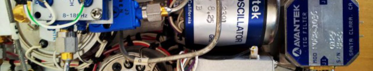
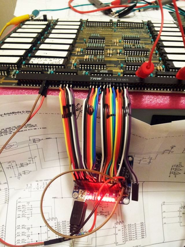
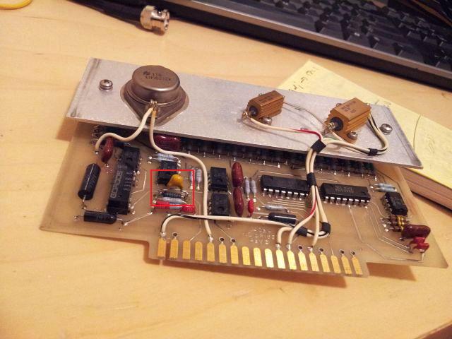
Some items of the mighty precision attenuator calibrator setup are still missing, like the automatic auto-zero/through calibration, and the adaption of the reflection bridge (see earlier post), but nevertheless, all parts are now in place to do some first real measurements (and generate, thanks to computer control, more data than anyone could have ever recorded manually, without getting close to nervous breakdown).

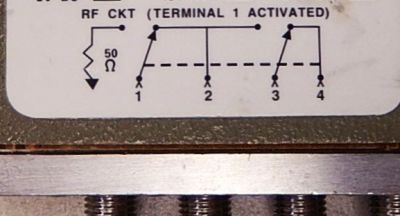
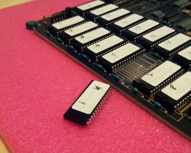
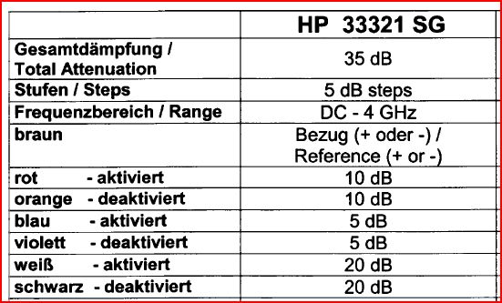
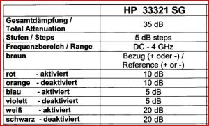
The device unter test (DUT). It is a HPAK 33321 SG step attenuator, 35 dB, in 5 dB steps – it is more or less a transmission line, with 3 resistor pads that can be individually switched in and out.
33321 sg step attenuator DUT

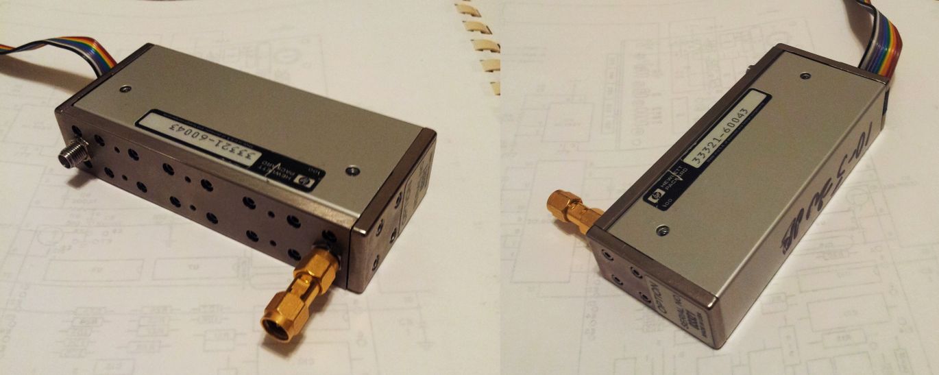
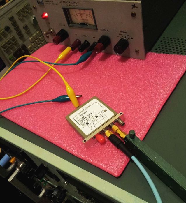
Also, note the SMA to SMA connector needed to get things connected vs. a through line. No allowance was made for this connector, it is a 18 GHz qualified precision part and will have very little loss.
hp 33321 sg data
As you can see, it is specified for 4 GHz operation – there are multiple models of these attenuators, both from Weinschel/Aeroflex and HP/Agilent/Keysight, up to 26.5 GHz or more. The 4 GHz models are relatively easily to come by, and others have claimed that these are actually quite usable up to higher frequencies. Let’s see.

While I don’t have exact specs for the 33321 SG model, there are similar models around, and typically, the numbers given by HP are +-0.2 dB at 10 dB, +-0.4 dB at 20, and +-0.5-0.7 in the 30-40 dB range. Repeatability about +-0.01 dB, which is quite impressive.

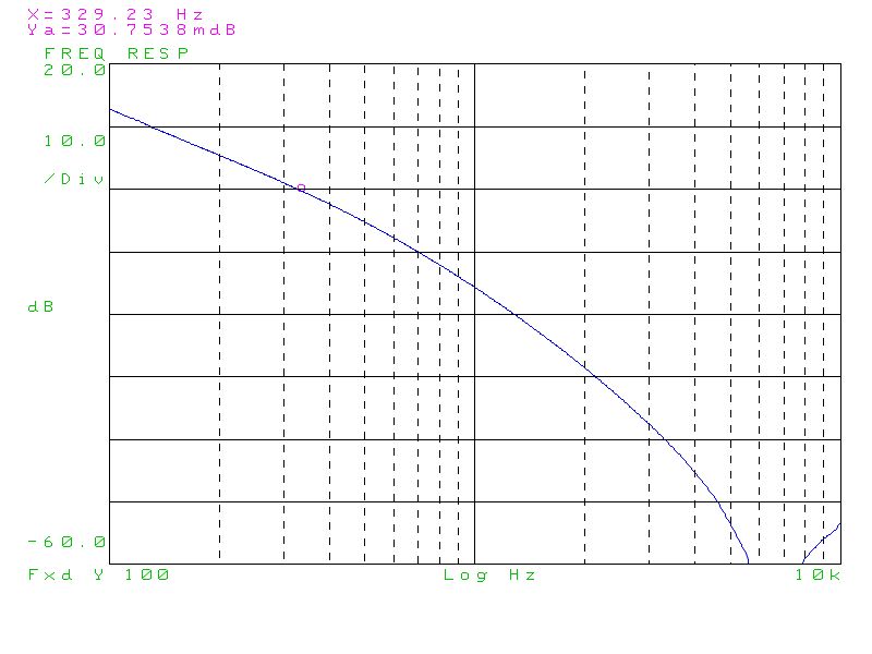
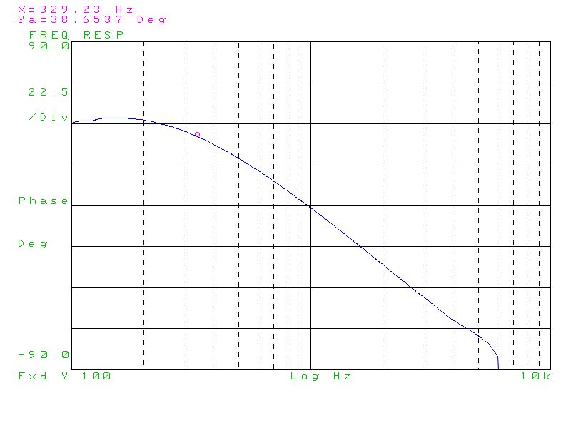
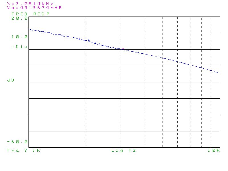
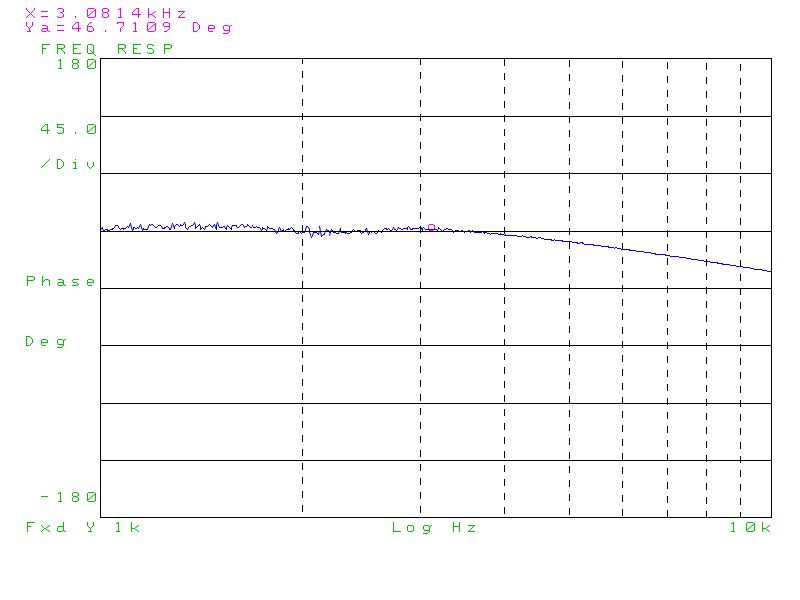
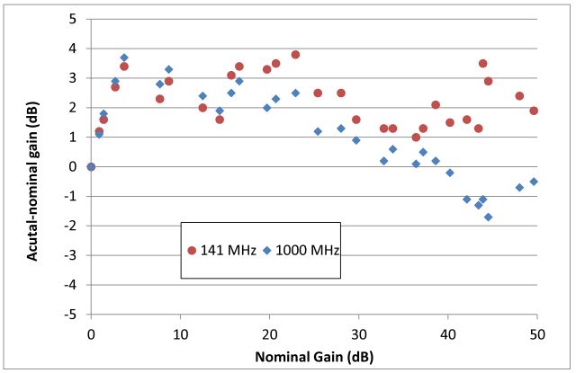
To be exact, we will be dealing with insertion loss here – not quite attenuation, but close, because no corrections have been made for any return losses (due to the SWR of the receiver and of the DUT, which might also change with attenuation setting).

Now, the test:

Step (1) – the system was calibrated without the DUT, just with the cables (from generator and to receiver) directly coupled (“through” calibration)
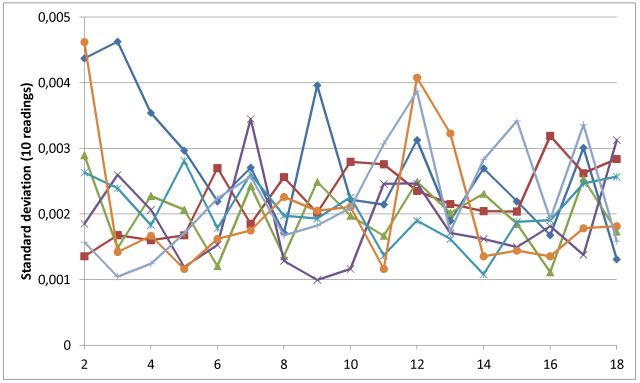
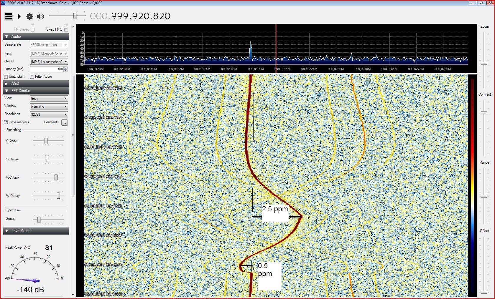
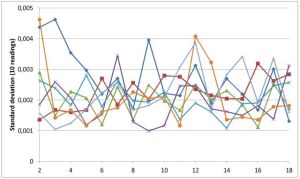
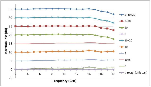
Step (2) – the attenuator was inserted, and tested at all the steps from 0 to 35 dB, 0 dB was measured twice. For all steps, 10 readings were taken, 1 per second, and averaged. Standard deviations are very small, showing the excellent short-term stability of the setup:
sdev vs frq at various attenuations

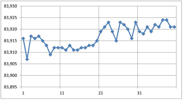
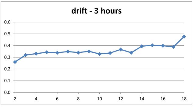
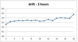
Step (3) – again, a through calibration. The measurements took about 3 hours – the drift was small, and distributed linearly with time over the measurements. Drift is pretty much independent of frequency. Later, there will be a drift correction anyway, by the yet-to-be-implemented auto-calibration feature.

Drift – 3 hours; about 0.1 dB absolute per hour.
drift in dB, 3 hours period

Insertion loss – at all the various steps, relative to “through” connection
insertion loss vs. through connection

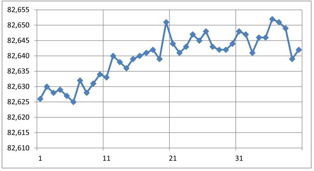
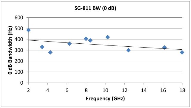
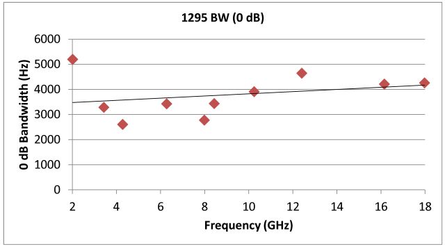
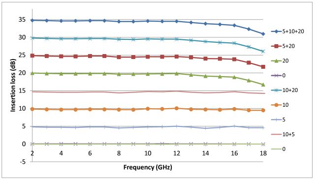
Insertion loss – relative to “0 dB” setting. This is relevant for most of the practical cases, where the 0 dB values are stored in a calibration ROM, and the levels corrected accordingly. Repeatability of the 0 dB setting was also checked – standard deviation is about 0.04 dB, but might be much better short-term (more like the 0.01 dB claimed in the datasheet). However, keep in mind, 0.04 dB at 10-18 GHz is not more than a few mm of cable movement, or a little bit more or less torque on a connector.

insertion loss (corrected for 0 dB loss) vs frequency

Deviation of 0 dB corrected loss from the nominal values (5-10-15-20-25-30-35 dB steps)
total insertion loss - 35 db to 0 db, 5 db steps - deviation actual-nominal

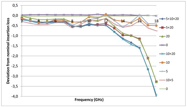
As you can see, the attenuator works great well above the 4 GHz, easily to 12 GHz. Still usable up to 18, with some error. This error seems to mainly come from the 20 dB pad. Rather than relying on just the 20 dB pad measurement, some maths were done on the data to determine the insertion loss difference (attenuator switched in, vs. switched out), for each off the pads, e.g., for the 20 dB pad, by subtractions of these measurements:

(1) 20 dB in, 5 and 10 out; vs 0 dB
(2) 5 and 20 in, vs 5
(3) 10 and 20 in, vs 10

So there are actually 3 combinations for each pad that allow determiation of the actual insertion loss, for each individual pad. Furthermore, this utilizes the 1295 received at different ranges of the (bolometer) log amplifier, and with different IF attenuators inserted – and will average out any slight errors of the log amp, and calibration errors of the IF step attenuators of the 1295. For even more cancelation, the source power could be varied, but fair enough.

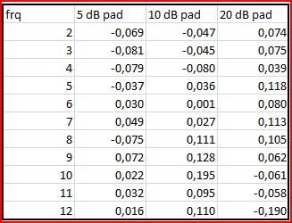
Results of a lot of (computerized) number crunching:

Insertion loss difference in vs. out, for each pad
attenuation of each pad vs frequency
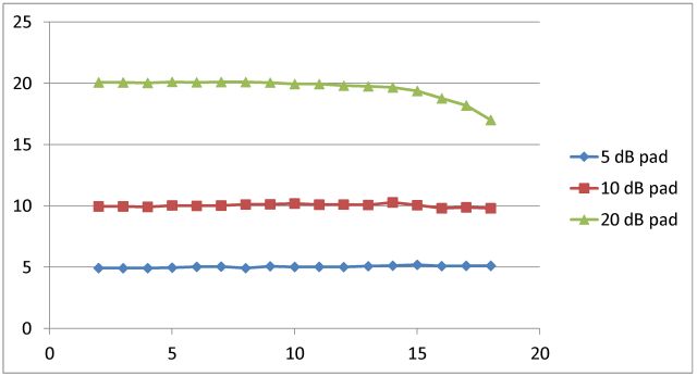
The 5 and 10 dB pads are performing great, the 20 dB pad – a bit less. Well, there must be a way to tune this a bit – but don’t have a cleanroom here, and the fixtures, to scratch a bit of resistive mass from the pad, at certain places, etc. Wonder how they do this at the factory, and if in fact there is some manual tuning, at least for the higher frequency units.

Deviation from nominal, for each pad
calculated attenuation for each of the pads - actual minus nominal

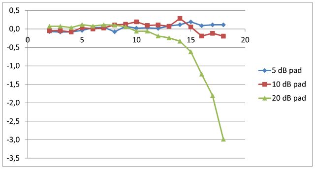
This is really a quite striking level of accuracy – much better than specification, and also indicates the level of precision already achievable with the still temporary attenuation calibration setup. Up to 12 GHz, no issues at all.
33321 sg pad in vs out values

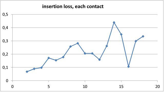
The 0 dB loss – some might be in the connectors, some in the transmission lines, some in the “through” switches of the 3 attenuators. Simply assuming that there aren’t any losses in the connectors and transmission lines, this is the loss per attenuator switch, when in “through”=”pad switched out” position.
0 dB insertion loss (calculated), per contact

All in all, the best way to use these attenuators obviously is to very accurately measure the 0 dB insertion loss, on a pretty narrowly spaced frequency scale. For the attenuator pads, these are best measured by recording values at various attenuations, and polynomial fits give very good approximation, without the need for a lot of density on the frequency scale, and seem to be merely additive, with little cross-correlation errors.
Sure, such things can all be analyzed with much more maths involved, but I doubt it will impact much the application-relevant aspects, and would be rather just a numerical exercise.

Micro-Tel 1295 receiver: parallel to serial converter – digital readout

The Micro-Tel 1295 has a GPIB (IEEE-488) interface, and in principle, can be fully controlled through this. In principle, but, not with ease; and, as it turns out, the build-in processor is running on 70s hardware, and doesn’t respond well to my National Instrument GPIB card. The only thing I need are the attenuation readings, in dB, same as shown on the front LED display.

Also, these GPIB cards are expensive, and I would rather like to control the whole attenuator calibration rig through one single USB port – also to be able to run in with various computers, not just with a dedicated machine.

In brief, after trying hard, I gave up – there need to be a more practical way to read the 1295 data.

First, how to get the data out, if not through the IEEE-488 interface? The case if fully closed, and drilling a hole, mounting a connector – NO. The modification should be reversible.
But there is a solution – the band selection connector, which is already used to remotely control the band switching, has a few spare pins!

This connector is a sight by itself:
micro-tel 1295 band control (and now serial output) plug amphenol wpi mini hex series 126

AMPHENOL/Wire-Pro “WPI” 9-pin “126 series” miniature hexagonal connector, 126-220; these connectors have been introduced in the 1940s, or latest, in the 50s. Still, available today… but the first piece of test equipment that I have ever seen that uses such kind of connectors. 500 Volts, 7.5 Amp – seems like a lot for such a small connector, at 14.99 USD each (plug only).

So, how to run the full display info over one or two wires? Update rate is 1 reading per second, or 1 reading every 4 seconds, not a lot of data – still it needs to be reliable, easy to use.
After some consideration, I decided to use a RS232 interface, with TTL level logic (rather than RS232 voltage levels-only using a short cable), and running it at 2400 bps, transmitting the data from the 1295 receiver to the main micro. This main controller, an ATmega32L can easily handle one more incoming signal, via its USART, and buffer any data coming from the 1295 before it is requested over the USB bus, by the PC software.

There are 5 full digits, plus a leading 1, a optional “+”, a leading-0 removing signal, and a blanking signal, which is set to low when the display is updating, or when the receiver is not giving a valid reading (over/underrange). Each digit needs 4 bits, binary coded decimal (BCD), so in total: 5×4+4=24 bits. Perfect match for the A, B, and C ports of a ATMega32L. This micro will monitor the blanking signal, and after sensing an updated display, read out the BCD information, convert it into a readable string, and send it out at the 2400 bps, via a single wire, no handshake, or anything. Will just keep on sending.

The easiest way to get the signal was determined to be directly at the display unit (A7) itself.
1295 a6 assembly schematic

There is also some space to fit the micro board, a commercial (Chinese, called “JY-MCU”, Version 1.4) ATMega32L minium board, with USB connection. These are really great, running at 16 MHz, with some little LEDs (which are on port B – disabled for this application), and a bootloader. It just saves a lot of time, and these boards are really cheap, below $10.

A 34 pin ribbon cable, with double row connector, salvaged from an old PC – so the controller/parallel-to-serial converter can be removed from the 1295 if no longer needed, and even the cable de-soldered.

The modified assembly
1295 a6 assembly top
MC14511 CMOS latches-BCD decoders-LED drivers – very common for 70s/early 80s vintage, and still working great!

1295 a6 assembly

Data is being transmitted, no doubt:
2400 bps signal

Now it is just a matter of some lines of code, and soon, some real insertion loss tests can start! Stay tuned.

PLL characterization – final results for the Micro-Tel SG-811 and Micro-Tel 1295 circuits

After some experimentation, measurements, etc. – as described before, time to wrap it up.

The PLL loop filter output is now connected to the phase lock input (the additional 1 k/100 n low pass in the earlier schematic has been omitted), with a 330 Ohm resistor in series. This will remain in the circuit, because it’s handy to characterize the loop, and to provide a bit of protection for the opamp output, in case something goes wrong, to give it a chance to survive.

With the charge pump current adjustments now implemented in the software, that’s the result, all pretty stable and constant over the full range.

The SG-811 signal source
micro-tel sg-811 pll bandwith vs frequency

The 1295 receiver
micro-tel 1295 pll bandwidth vs frequency

Micro-Tel SG-811 PLL: frequency response
Gain
sg-811 final gain

Phase
sg-811 final phase

Micro-Tel 1295: frequency response
Gain
1295 pll final gain

Phase
1295 pll final phase

PLL frequency response measurement: a ‘not so fancy’ approach, for every lab

Measuring gain and phase shift of some decice doesn’t seem like a big deal, but still, how is it acutally done? Do you need fancy equipment? Or is it something of value for all designers of PLLs that don’t just want to rely on trial and error?

The answer – it’s actually fairly easy, and can be done in any workshop that has these items around:

(1) A simple function generator (sine), that can deliver frequencies around the band width of the PLL you are working with. Output level should be adjustable, coarse adjustment (pot) is enough. You will need about 1 Vpp max for most practical cases.

(2) A resistor, should be a considerably lower value than input impedance of the VCO. Typical VCOs might have several 10s of kOhm input impedance. Otherwise, put a unity gain opamp (e.g., OPA184) in between the resistor and the VCO tune input.

(3) A resistor, and some capacitors (depends a bit on the bandwidth), for general purposes 10-100 kHz, a parallel configuration of a 100n and 2.2 µF cap is just fine. In series with a resistor, a few kOhms. This network is used to feed a little bit of disturbance to the VCO, to see how the loop reacts to it… the whole purpose of this exercise.

(4) Make sure that the loop filter has low output impedance (opamp output). If your circuit uses a passive network as a loop filter, put in an opamp (unity gain) to provide a low output impedance.

(5) A scope, any type will do, best take one with a X-Y input.

Quick scheme:
pll gain phase measurement diagram

To perform the acutal measurements, the setup is powered up, and phase lock established by adequately setting the dividers, as commonly done.
The signals (X: drive=input to the VCO, Y: response=output of the loop filter) are connected to the scope. Set the scope to XY mode, AC coupled input, and SAME scale (V/div) on X and Y.

Next, set the signal gen to a frequency around the range of the expected 0 dB bandwidth (unity-gain bandwidth), and adjust the amplitude to a reasonable value (making sure that the PLL stays perfectly locked!). Amplitude should be several times larger than the background, this will make the measurements easier, and more accurate. If you have a spectrum analyzer, you can check for FM modulation. On the Micro-Tel 1295, which has a small ‘spectrum scan’ scope display, it looks like this:
1295 fm modulated signal during gain-phase test

On the X-Y scope display, depending on where you are with the frequency, it should show the shape of an ellipse, somewhat tilted – examples of the pattern (“Lissajous pattern”) below.

Frequency lower than 0 dB bandwidth – in other words, the loop has positive gain, therefore, Y amplitude (output) will be larger than X (input)
pll gain phase measurement - positive gain (frequency below BW)

Frequency higher than 0 dB bandwidth – in other words, the loop has negative gain, therefore, Y amplitude (output) will be smaller than X (input)
pll gain phase measurement - negative gain (frequency above BW)

And finally, same signal amplitude in X and Y direction.
pll gain phase measurement - 0 dB condition

Sure enough, you don’t need to use the X-Y mode, and circular patterns – any two channel representation of the signals will do, as long as their amplitude is measured, and the frequency identified, at which X and Y have equal amplitude (on the X-Y screen, also check the graticule, because the 45 degrees angle is not so easy to judge accurately). That’s the unity gain (0 dB bandwidth) frequency we are looking for. With little effort, the frequency can be measured to about 10 Hz.
The X-Y method has the big advantage that it relies on the full signal, not just certain points, and triggering a PLL signal with a lot of noise can be an issue.

Try to keep the amplitude stable over the range of frequencies measured – by adjusting the signal gen.

Ideally, the 0 dB bandwidth is measure at various frequencies over the full band of your VCO, because the bandwidth can change with tuning sensitivity, etc., of the VCO.

The 0 dB bandwidth is not the only information that can be extracted – also the phase shift is easily accessible. Just measure, at the unity gain frequency, or any other frequency of interest for you, the length of the black and red lines:
pll gain phase measurement - 0 dB condition - phase determination

The phase angle is then calculated by: divide length of red line, by length of black line, in this case, 4.6/6.9 units. Then apply the inverse sin function, to get the phase angle, sin^-1(4.6/6.9)=41.8 degrees. The 0 dB frequency, in this case, was 330 Hz.

A quick comparison with the data acquired using a more sophisticated methods, a HPAK 3562A Dynamic Signal Analyzer.

Gain: 0 dB at 329 Hz – that’s close!
pll test result - gain

Phase: 38.7 degrees – fair enough.
pll test result - phase

A proper PLL setup should provide at least 20 degrees of phase shift (note that this is not the so-called phase margin, which is a property of an open loop). Closer to 0 degrees, and the loop will remain stable, but a lot of noise (phase noise) and osciallation, finally, occasional loss of lock will be the result.

It’s also a good idea to check that the gain function drops off nicely – there are certain cases, where mulitiple 0 dB points exist – you need to look for the 0 dB point at the highest frequency.

Any questions, or if you need something measured, let me know.

Fractional-N PLL for the Micro-Tel 1295 receiver: some progress, more bandwidth, two extra capacitors, and a cut trace for the SG-811

Step 1 – Programming of the ADF4157, no big issue – fortunately, all well documented in the datasheet. The 1.25 MHz phase detector frequency selected will allow tuning in integer-only (no fractional divider) 10 MHz steps (considering the :8 ADF5002 prescaler).

One sigificant difference to the ADF41020 – the ADF4157 uses 16 steps for the charge current control (0=0.31 mA to 15=5.0 mA).

Step 2 – Checking for lock at various frequencies – in particular, at the low frequencies – the thing is running really at the low edge, 250 MHz input for the ADF4157. However, despite all concerns, no issues, prescaler and PLL are working well even at the low frequency. Quite a bit of noise! Not out of focus…
1295 noisy signal

The PLL is locking fine, but still, significant noise in the loop, and also visible in the 1295 scope display, with a very clean signal supplied to the receiver… bit of a mystery. When the PLL is disengaged, and the 1295 manually tuned – no noise, just some slow drift.

Step 3 – Increased loop bandwidth to about 8 kHz, even more noise – seems to PLL is working against a noisy FM-modulated source…. a mystery. Checked all cables, nothing is changing when I move them around.

Step 4 – Some probing inside of the 1295, and review of the signal path for the PLL tune and coarse tune voltages. And, big surprise – there is a relais (K1) on the YIG diver board, and this disengages a low-pass in the coarse tune voltage line – it is a 499k/22 µF RC, several seconds time constant.

See the red-framed area:
micro-tel 1295 A3B9 YIG driver loop damping

Tackling this through a lowpass in the coarse tune feed line (from the coarse tune DAC) didn’t change a thing – the noise is getting into the YIG driver from instrument-internal sources, or partly from the opamp (U5, LM308) itself, when it is left running at full bandwidth. As a side comment, note the power amplifier – it is a LH0021CK 1 Amp opamp, in a very uncommon 8 lead TO-3 package. Hope this will never fail.

Usually, I don’t want to modify test equipment of this nature, because there is nothing worse than badly tampered high grade test equipment. All conviction aside, 2 X7R capacitors, 100 n each, were soldered in parallel to the R38 resistor, so there will be some bandwidth limitation of the YIG driver, even with the K1 relais open.
micro-tel A3B9 YIG driver board - modified

With these in place – the noise issue is gone.
1295 clean signal

Now, triggered by this discovery – the SG-811 uses a very similar YIG driver board, which also has a low pass engaged, in the CW mode – however, not in the remotely controlled CW mode, with externally settable frequency… easy enough, just one of the logic traces cut, and now the filter stays in – don’t plan on sweeping it with a fast acting PLL anyway.

Back to the fractional-N loop: after some tweaking, the current loop response seems quite satisfactory. Set at 3 kHz for now, with plenty of adjustment margin, by using the 16-step charge pump current setting of the ADF4157. Getting 45 degrees phase margin (closed loop) at 3 kHz – therefore, should also work at higher bandwidth. Will see if this is necessary.

PLL gain
1295 fractional-n loop mag

PLL phase
1295 fractional-n loop phase

R820T, RTL2832U SDR USB stick: some more findings about temperature sensitivity.

Another hack you can do with the SDR USB sticks – mount the clock crystal (28.8 MHz) remotely, feed a stable RF signal at any frequency you desire, and use it a as a thermometer. This will work great at room temperature and up to about 50 deg C, but beware, the ready will be ambiguous at higher temperatures. Here is a quick experiment:

Signal was supplied at 1000 MHz, from a virtually perfectly stable source. At some point, the crystal was touched with a finger (making sure not to touch any of the traces or components, as this could capacitively affect the oscillator). Surprisingly, the frequency first goes down (-0.6 ppm), and then up (+2.5 ppm).
temp effect (hot to cold to hot) ppm

Why is this so surprising – let’s have a quick look at typical crystal oscillators, there are several types, AT-type (most common), SC-type, and closely related IT-type, and others, less common. Nearly exclusively have I come across AT-type so far, for all kinds of cheap clock application. AT type means: inversion point at room temperature, then the frequency decreases a bit with temperature, to about 60 degrees C, then it increases again. See the black curve in this diagram (note that the absolute values are just typical, arbitrary, and change with cut angle tolerance):
r820t quartz ref osc temp dependence
Red line shows the typical characteristics of a SC (or IT)-cut crystal.

Rather than the expected AT-typical transition through a minimum frequency, when going from about 60-70 deg C, down to 35 deg C (body temperature), we observe just the opposite behavior (more like SC-type) – reference frequency goes through a maximum (which is a minimum of the shown signal frequency, if the signal is a constant 1000 MHz).

So it seems, the manufacturer did actually consider a relatively high operating temperature of this device when selecting the crystal, which is running at about 60 degrees – just the rough temperature of the board/crystal.
An AT-type would have been much counter-productive, because this is optimized for constant frequency over a broad range of temperatures, say, -10 to 60 deg C. However, for the SDR USB stick, the temperature related frequency change should be minimal at and around the hot operating condition of the board – I don’t think this is just coincidence, but somebody acutally put some thought into getting a device frequency stable, without any ovens or other compensation devices.

R820T, RTL2832U SDR USB stick: gain accuracy tests

The R820T has the nice feature of a build in pre-amplifier, 0 dB to 49.6 dB nominal gain. Now, the question is, with all the nominal values, what is the acutal gain, and how does this change with frequency?

With the established setup, the frequency-stabilized SDR USB stick (28.8 MHz supplied by a HPAK 8662A, at 500 mV level), and the 8642B source, the gain of the R820T was set to the various values, step by step, and the RF input level varied to keep the SDRSharp FFT peak level at exactly -25 dB. The -25 dB reading can be taken to about +-0.2 dB, when looking at the FFT display.
The test was carried out at two frequencies, namely, 141 MHz and 1000 MHz. Don’t do such evaluation anywhere close to multiples of 28.8 MHz – there are some reference-related spurs that can affect the accuracy.

First, the RF input power needed to get a -25 dB reading:
r820t rf input power at -25 dB vs nominal gain
Interestingly, at 0 dB gain, a bit more power is needed at 141 MHz to get -25 dB, which means, the R820T is a little bit less sensitive at 141 MHz than it is at 1000 MHz, but only at the 0 dB gain setting. At higher gains, the data are more or less superimposed.

Note also that the 43.9 dB and 44.5 dB gain settings have actually identical gain! No idea why.

r820t acutal gain vs nominal gain
These are the acutal gains, calculated from above data, vs. the nominal gain. Pretty linear, but clearly some positive deviation at the low gains.

The full dataset:
r820t rtl2832u sdr usb gain check

This is even more clearly visible in the deviation plot:
r820t gain error vs nominal gain

Accordingly, the preamp provides a bit more gain at lower frequencies, say, 141 MHz, especially when set to high gain, above 35 dB nominal. Below 35 dB, gains for 141 and 1000 MHz are virtually identical.

If you have a SDR USB stick of a different type, and want to have some gains-levels etc measured, just let me know! I might be interested.