R820T, RTL2832U: narrow-range linearity

Some more linearity tests, now over a narrow range, with a precisely linear and calibrated source, measured at 1000 MHz, otherwise all the same is in the earlier post.

These tests were done at a 0 dB gain setting, and the input power was varied in 1 dBm steps.
r820t gain linearity (narrow range)

r820t linearity deviation (narrow range)
The results speak for themselves – the SDR USB stick is pretty accurate, if you want to do a relative comparison of power levels over a range of 10 dB or so. Accuracy might be in the range of +-0.5 dB, or better, provided that the slope has been determined for a given gain setting (don’t change the gain settings, if you need to do accurate measurements). If you want to measure insertion loss, the best way would be to vary the source power in calibrated steps (by a 1 dB high precision attenuator), and just use the SDR USB at a constant dB reading, over a narrow range of +-1 dB, then your measurement error will be limited to virtually the precision attentuator error only. For such tests, it is always good practice to have a 6 dB or 10 dB attenuator at the SDR USB input, to avoid artifacts caused by the non-negligible return loss (SWR) of the SDR USB stick input.

An open item – to go further, one would need to check linearity at various frequencies of interest, etc., but this is all beyond the scope of the SDR USB stick – if it comes to below 0.5 dB accuracy, that’s something better done in a cal lab anyway, nothing that is necessary too frequently out in the field.
For comparison, with a high precision dedicated level measurement receiver (like the Micro-Tel 1295), achievable relative level accuracy (not linearity) over 10 dB is about 0.03-0.05 dB – over a much wider frequency range. Also note that most commonly available spectrum analyzers (Rigol, etc.) aren’t all that linear, see their specs.

R820T, RTL2832U SDR USB stick: using it as a “poor man’s” spectrum analyzer – level linearity, level accuracy

There are some good reasons to always carry one of the SDR USB sticks around – it’s a great little spectrum analyzer. But hold, what does it have in common with the purpose build-professional analyzers selling for USD 1k or more? It certainly has one particular advantage, the SDR USB stick is very small, a mere 10 gramms, and only needs about 1 Watt of power. And it covers the full span of frequencies of general interest (at least is you add an upconverter, for low frequency and HF stuff below 24 MHz).

Well, what are some key requirements of a good spectrum analyzer?

(1) No spurs, at least no unpredictable ones. Well, there are spurs, but mainly multiples of 28.8 MHz (reference), and some spures related to the sampling frequencies (always check if the spur changes, by checking out several sample rates that are not multiples of each other)

(2) Intermodulation distortion. More complicated, will be analyzed later.

(3) Low input return loss (otherwise, amplitudes will be inaccurate). Will be measured later, the VNA rests back home in Germany. But this limitation can be easily overcome by putting a 6 dB attenuator in front of the SDR USB.

(4) Frequency accuracy – this is not great, but stable within a few ppm. If you want to add a precision reference, see earlier post.

(5) Amplitude accuracy – it needs to be very linear (i.e., a 1 dB step in signal strength must convert to a 1 dB step on the readout, same for 10 dB steps, etc.), and this should not very too much with frequency. Absolute amplitude accuracy (i.e., if 1 dBm is fed into the RF input, it needs to read 1 dBm power) – not applicable to the SDR USB stick, it only shows power in nominal, un-calibrated dB.

Well, let’s tackle item 5, and work out some absolute calibration.

The R820T tuner of the SDR USB stick under consideration here has a build-in preamp. This has nominal gains from 0 dB, to 49.6 dB. Some gain curves have been reported for other SDR USB sticks elsewhere, let’s do some in-depth analysis.

How to get this measured properly? The setup and method:
With 1.024 MSPS, 65536 FFT bins, RF frequency of 1000 MHz (HPAK 8642B), reference at 28.80 MHz – 500 mV (provided by an HPAK 8662A) and gains set to values of 0 dB, 20.7 dB (about mid-range), and 49.6 dB (max gain), the input RF power (which is calibrated in absolute dBm, and fed to the SDR USB stick by a low-loss cable) is varied in 10 dB steps, and the dB reading taken from the SDRSharp FFT spectrum display. Note that fully accurate reading of the dBs is only possible if the frequencies (reference and signal) are dead-stable, otherwise everything will be drifting up and down, and the FFT bins won’t be in the same place all the time.

Here are the results:
r820t db output vs rf power input at various gains
Everthing is quite linear (a good fit with just a line), but you notice, the slope of the lines change a bit, depending on the gain setting. In other words, a 1 dBm chain will not always result in an exactly 1 dB change on the SDSSharp display, at high gain setting, it will almost fit, at 0 dB, there is only about 0.93 dB change (readout) for every 1 dBm power change at the input. Well, over 40 dB, that’s an error of about 3 dB, not much, but more than desirable.
r820t level accuracy

After some more measurements, at 38.6 dB nominal gain, it relationship of level slope vs. gain seems pretty clear, at least at 1000 MHz.
r820t linearity (slope) vs nominal gain

After applying the slope correction (comparing a linear fit, with the acutal measured data), these are the residuals:
r820t linearity deviation (wide range)
Less than 1 dB – that’s within the measurement error of the calibration apparatus!

Next interesting item for practical use, the RF input power needed to get a 0 dB reading – the absolute power calibration for this SDR USB stick. This seems to vary from stick to stick only by 2-3 dB, but I don’t have a big set of sticks, multiple lots etc. – so this might be shifted depending on the exact device you are using, but trends should be the same, for all R820T sticks.
r820t 0db equivalent rf input power vs gain
According to this diagram, for any measurements above -40 dBm, you need a good set of attenuators, to bring the signal level down. In fact, the SDR USB might actually make a very decent subtitution type attenuation test receiver, if you put it in line with a precision attenuator, and only use a few dBs of span of the SDR USB (well-calibrated) to determine the signal levels. I checked quickly for drift of the level calibation vs. R820T temperature – there doesn’t seem to be any strong effect, which is a good sign that there is no need to re-calibrate the levels all the time.

R820T, RTL2832U SDR USB stick – sensitivity, dynamic range

After looking around in the web, there doesn’t seem to be a whole lot of information out there on the sensitivity and dynamic range of the SDR USB devices, at least not for the type I’m using here. Even the R820T datasheet isn’t all that clear – there are various versions of the R820T, also using different clock frequencies, with 28.8 MHz, being the most popular lately.

Therefore, time for some measurements.

The setup:

(1) HPAK (formerly HP, then Agilent, now Keysight) 8662A Signal Generator as the reference source, 28.800 MHz, 500 mV level.

(2) HPAK 8642B Signal Generator as the test signal source. This has a calibrated output from -140 dBm to +20 dBm, and very clean and free of spurs, and provides up to 2.1 GHz.
Absolute amplitude accuracy is about 1 dB, linearity is considerably better. As it says on the instrument cover – 70 pounds, “two person lift”.
The 8642B is phase locked to the 8662A clock, via a common 10 MHz reference signal. So even with drift, there can’t be any frequency errors getting into the way of our precision testing.

(3) Some well-shielded test cables, RG223/U, and adapters to link to the MCX connector (use a good test cable, but not your best – most of the SMA to MCX connectors aren’t all that precise, and may damage precision SMA connectors).

(4) The modified SDR USB stick, see earlier post.
r820t rtl2832u sdr usb dut

(5) Laptop PC, running SDRSharp. 1.024 MSPS, all automatic gain and frequency adjustments disabled, I/Q correction enabled.

r820t rtl2832u sdr usb test setup

First, the sensitivity check. Tuned the SDR USB to various frequencies, and measured the input power (dBm needed to get a -40 dB reading, at max gain of the SDR USB – 49.6 dB nominal), this is about 15 dB above the noise floor, and still a signal level that is very stable and can be accurately measured. Afterwards, set gain to 0 dB, and increased RF input power until 0 dB reading was obtained – this is the maximum power that can be reasonably fed to the SDR USB (no damage will occur up to +10 dBm; and even +20 dBm doesn’t seem to do much, at least not if only applied for a short time).

Power levels for -40 dB reading at max gain, and 0 dB reading at 0 dB gain:
r820t input sensitivity and max power
Sensitivity is quite constant over a pretty large range, up to 1500 MHz, no problem. Lowest frequency the thing can handle is about 24 Mhz (doesn’t tune any lower). Note that there are some spurious signals present around 28.8 MHz, (internal) ref clock leakage, and its 2nd harmonic.
R820T usb sdr dynamic range and sensitivity

The RF input power (about -130 dBm) to get -40 dB amplitude, at max gain of the SDR USB, this is quite remarkable, and still about 15 dB above the noise floor. So the R820T exhibits very high sensitivity, no doubt.
Here is an estimation of the dynamic range – “useful” because, it is still has some margin for noise. For the full dynamic range, add about 15 dB.
r820t sdr usb dynamic range
About 93 dB (108 dB full range, from noise floor, at 49.6 dB gain, to 0 dB at 0 dB gain).

R820T, RTL2832U: SDR USB stick hack – clean and stable reference!

One of the shortcomings of these handy and cheap SDR USB sticks is the offset of the reference, and the drift. First, lets see what we have: in the meantime, I have two more or these little units to play around, and all have about 70-100 ppm offset, positive.
The reference is derived from a small 28.8 MHz crystal, and while such crystals are pretty much suitable for clock generation, they do drift with temperature, and the SDR USB stick is getting hot during use… Quick look inside (case can be easily opened, no damage):

r820t sdr usb stick opened
The small silvery metal can is the crystal. Any temperature change will cause this to slightly change frequency.

So, what about the crystal drift? Easy enough, just hooked up one of the sticks to a counter (with stable timebase; you need to use high impedance probe, otherwise, proble will pull the crystal frequency), and logged the frequency values for an hour, after “cold” startup (stick with no case).
The result:
r820t ref clock drift
1 to 2 ppm, that’s not all that bad! Still, in the world of precision oscillators, it’s ridiculously drifting. So for any precise characterization of the SDR USB device, we need to get this under control. Some have tried to replace the crystal by a TCXO, but even with this, it will be challenging to break the 1 ppm (1 kHz at 1 GHz!) mark.

A quick look at the datasheets reveals that pins 8 and 9 of the R820T are the input/output of the xtal drive circuit, and pin 10 forward the clock signal to the RTL2832U, to safe some parts, and cost.

That’s how the oscillator output looks like, probed at pin 9, with a 10 Meg probe (0.5 V/div, 10 ns/div)
r820t ref clock signal 0.5 v-divy 10 ns-divx
The signal, amplitude is about 1.5 Vpp, with a DC bias of 1.2 V.

Therefore, if we want to substitute the crystal, we have to feed a few dBms of power at 28.8 MHz into pin 8, and leave pin 9 unconnected. The feed line (50 Ohms) requires some adequate termination. We also need to provide a DC block, with a little coupling capacitor.
That’s the little hack:
r820t sdr usb ref clock hack
A SMC connector, terminated with 82 Ohm (which will be in parallel with the impedance of the R820T, hopefully giving about 50 Ohm, or close enough), and with 0805 10 nF capacitor, connected to pin 8 of the R820T.

As for the new reference source – nothing less than a HPAK 8662A, which is a real marvel of engineering and one of the best sources I can suggest for any tests that require low phase noise close to the carrier. It is stable to better than 0.0005 ppm, per day – compare this to the 1 ppm, per hour…..
Sure, not the mention – the 8662a carries 80 pounds of electronics, a big fan, and uses about 300 Watts of power to keep things clean.

The new clock source for the SDR USB stick:
r820t new clock source 8662a

The reference level needed to drive to R820T oscillator – just by trial and error, things start to work at about 400 mV, and up to 1 V of signal doesn’t seem to change anything. So I set the level to 500 mV into 50 Ohm, and this seems to work well.

Interestingly, the R820 T seems to work from about 28.75 to 28.85 MHz reference, with no change in performance (at least nothing obvious), except, of course, for the frequency shift. At frequencies below about 28.72, and above 28.89, the stick crashes-no more data comming.

Some tests: 28.800 MHz reference, 1 GHz signal (note the small frequency shift, which is related to SDRSharp software, not to any hardware offsets)
28800

28.75 MHz reference – still 1 GHz signal
28750

28.85 MHz reference – still 1 GHz signal
28850

Checking the math, this all makes sense – for 28.75 MHz, a reading of 1001.739 MHz would be expected, and 998.267, for the 28.85 MHz reference.

PLL measurements continued… ADF41020 locking the Micro-Tel 1295

With the work on the Micro-Tel SG-811 generator PLL mostly completed, some trials with the Micro-Tel 1295 receiver – this instrument has similar YIGs fitted, just needs to be tuned 30 MHz above the actual frequency tuned, because the 1295 is running on a 30 MHz IF (all diagrams have tuned frequencies, not LO frequencies).

After some crude analysis of the schematics, the 1295 seems to be able to handle a bit more PLL bandwidth – so the target set more in the 500 Hz to 1 kHz region, and some calculations were carried out with the ADIsimPLL program, to determine the rough capacitor and resistor values – otherwise, the loop filter is the same as for the SG-811 PLL, also using an OPA284 opamp.

Otherwise, pretty much comparable results (earlier post related to the SG-811), for example (17.8141 GHz tuned/17.8171 GHz LO frequency, Icp setting 6):

Gain (disregard 1 to 10 Hz)
micro-tel 1295 17814100 kHz cpc6 gain

Phase
micro-tel 1295 17814100 kHz cpc6 phase

After quite a few of these measurement (doesn’t actually take too long), the results.
adf41020 pll bw phase margin 1295

Phase margin vs. bandwidth
pm vs bw adf41020 micro-tel 1295

Bandwidth vs. charge pump current Icp setting, at various frequencies
bw vs icp at various frq adf41020 micr-tel 1295 pll

Again, a bandwidth frequency^0.7 product could be used to get the numbers down to two parameters – slope and intercept of the bandwidth*frequency^0.7 vs. Icp setting curve.
Finally, suitable Icp settings for a 600 Hz target BW:
bw vs frq adf41020 micro-tel 1295 with Icp adjustment

The result seems quite satisfactory, pretty much constant 600 Hz BW can be achieved over the full 2 to 18 Ghz range, at about 47 degrees phase margin. This should allow for stable operation. No locking issues were observed at any of the frequencies, even with full Icp current.

Fractional-N PLL for the Micro-Tel 1295: ADF4157/ADF5002

After spending most of the day at the beach, some more experimentation – with a fractional-N approach. Two little chips were around from another project, why not give it a try:

(1) The Analog Devices ADF4157, 6 GHz, 25 bit fixed modulus fractional-N PLL – this part is really great, for many purposes. It’s more or less pure magic what these folks at Analog do and achieve.

(2) To make it work up to 18 GHz, a prescaler is needed. Well, unfortunatly, I only have a :8 prescaler (ADF5002) around – this will give 0.25 to 2.25 GHz, for the 2 to 18 GHz input. Not quite ideal, because at 2 GHz it’s getting really into low frequencies for the ADF4157, and the output power of the ADF5002, which is a more-than-sufficient -5 dBm in the 4 to 18 GHz, range, but dropping off to only about -10 dBm at 2 GHz. At the same time, RF input sensitivity of the ADF4157 drops considerably for input frequencies below 0.5 GHz… we will see.

Some calculations:
With a 10 MHz reference clock, and the phase detector frequency set to 1.25 MHz (reference divider=8), this will result in 10 MHz steps, with 2^25 spacings in between. This gives about 0.298 Hz resolution. And moreover, with this setting, 10 MHz steps are possible, with no fractional-N divisor (which can always lead so some rather unpredictable fractional-N spurs).

The circuit – there is no big secret to it, a 5k1 reference resistor to set the charge pump current to 5 mA, and a few 6k8 resistors (0805 SMD) to make the chip compatible to a 5 V digital world. Two SMA connectors – one for the signal, and one for the 10 MHz reference. All wiring is done with 0.08 mm tinned copper wire… hope you have a steady hand. With a drop of epoxy glue, everything is held in place and well-protected.

20140903_223309

20140903_223233

Tests will follow – currently the loop bandwidth tests are running for the 1295, with the ADF41020 PLL.

Noise and spurs, ADF41020/Micro-Tel SG-811 PLL

After getting things worked out with the loop filter, some quick check for spurious responses. To do such analysis near the noise level, a FFT/dynamic signal analyzer can be used, but I find it somewhat troublesome, and rather use a swept frequency analyzer for any such work that goes beyond 1 kHz. Below 1 kHz, the FFT is hard to beat. One of the few exemptions is the HPAK 3585A spectrum analyzer, which covers from about DC to 40 MHz, and has resolution bandwidth filters of down to 3 Hz (discrete hardware, not software filters), with baseline at -135 dBm, or lower.

The 3585A doing its thing…
20140902_214758a

The results – 1 to 500 Hz
348_00_0001 to 05
Mainly 60 Hz harmonics – well, will need to keep the cables short (especially the coarse tune cables) and everything far away from mains transformers.

10 Hz to 5 kHz
348_00_001 to 5
Signal at 1 kHz is about -70 dBm, not much. No spurs.

5 to 30 kHz
348_00_5 to 30
Two unexpected spurs – 1st: 19.986 – this is an artifact of the 3585A. 2nd: 18766, this seems unreleated to the PLL (doesn’t change with frequency or divider settings), maybe some switchmode supply stray. Well, down below -100 dBm.

25 kHz (with some 60 Hz harmonic sidebands, -115 dBm) – reference spur, about -93 dBm.
25 khz spur detail

All in all, with some refinement of the software, and a bit of mechanical work to get this all mounted into a nice case, the setup should work find and provide great service.
Sure enough, some direct phase noise measurements on the SG-811 output will eventually follow, once the opportunity is right and the equipment at hand.

Micro-Tel SG-811/ADF41020 PLL: working out the details – loop filter, bandwidth, charge pump currents

Designing a stable PLL is not really a big challenge, with all the simulation tools available, and after you have mastered some basic experiments with the 4046 chip, or similar circuits. For PLL simulation software, I suggest to look at ADIsimPLL, available free of charge, from Analog Devices.
However, stable doesn’t necessarily mean wideband, and exhibiting similar characteristics over a full 2 to 18 GHz band. That’s what we want to achieve here.

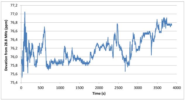
First some targets – after reviewing the circuits of the Micro-Tel SG-811/1295, and looking at the stability of the build-in YIGs, I figured that a good PLL bandwidth for this system would be somewhere in the 200-500 Hz region. This would still allow to correct for some mains-induced frequency fluctuations (50/60 Hz), and the frequencies are well below the 25 kHz phase detector frequency used for the ADF41020. Furthermore, the bandwidth should be reasonably stable of the full range of frequencies, with no need to use multiple loop filters, or troublesome switchable capacitors/variable gain amplifiers – all should be operated from a single-ended 15V power supply, to provide 0-10 V for the Micro-Tel 1295, and 0-3 V for the SG-811, from a single little board.

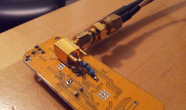
With this in mind, an OPA284 rail-to-rail precision amplifier (low noise, 4 MHz BW, can drive +-6.5 mA) was selected as the active part, and some capacitors (only use good quality capacitors, polymer dielectric, or stable ceramic capacitors, NPO) and resistors put together. There is only one adjustment, the damping resistor in the feedback loop.

Sketch of the schematic
adf41020 sg-811 pll loop filter

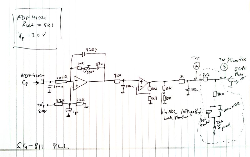
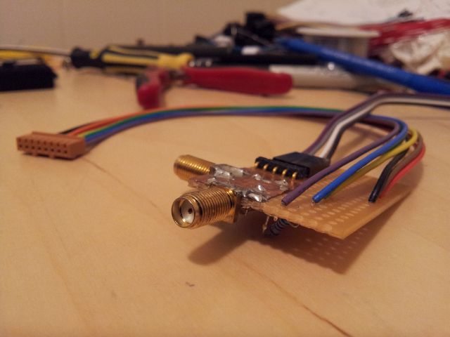
How to figure out the loop characteristics? Many pages have been written about this, determining open-loop gains and phase margins, etc., but how to approach this in practice, one you have done the calculations and figured out a setup that basically works? This is where the extra resistor and the two test points (A, B, see schematic) come into play. The resistor close to the output (8k2, this is just a temporary part, only inserted during test – bridged with a piece of view during normal operation) is used to isolate the loop output, from the SG-811 phase lock input (which is nothing else than a heavy VCO=voltage controlled oscillator). A few extra parts are also connected to feed a test signal to the VCO, in addition to the loop filter output voltage.
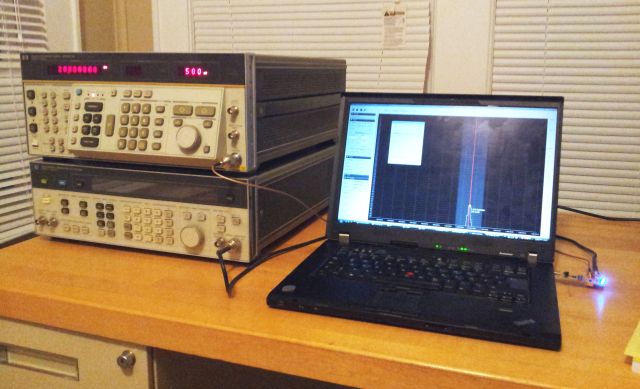
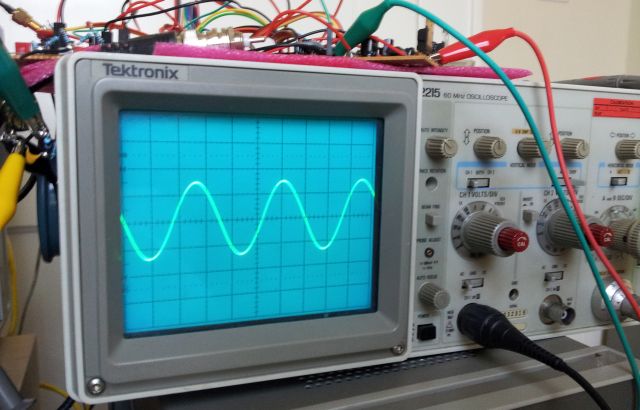
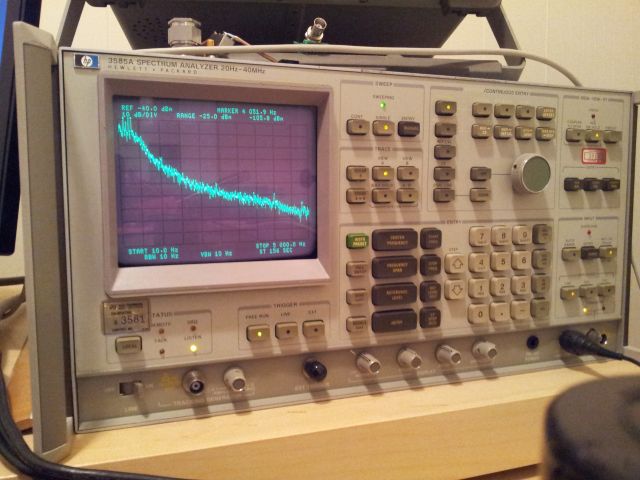
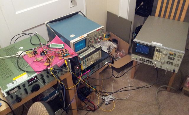
This test port is intended to disturb the PLL just a bit, without causing loss of phase lock, and measure the response. Such work is best done with a dynamic signal analyzer – I’m using a HPAK 3562a, not because it is the latest model, but because that’s what I have around here in my temporary workshop. It had the old CRT replaced by a nice color LCD screen, and it features a very acceptable noise floor, and gain/phases analysis.

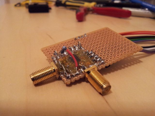
The test setup (please excuse the mess, not too much empty bench space around here)
pll loop test - micro-tel sg-811 - adf41020

Now we just need to work through various frequencies and settings, to better understand the characteristics of the system.
To cover all the YIGs and bands of the SG-811 (which might have unknown variations in tuning sensitivity, noise, etc.), frequencies around 2, 6, 10, 12.5 and 17.5 GHz were chosen for the test (exact values can be found in the worksheet, better not to use even values, e.g., 2.0000 GHz, but to exercise the divider circuits – to see if there are any spurs).

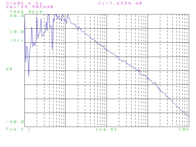
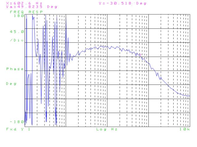
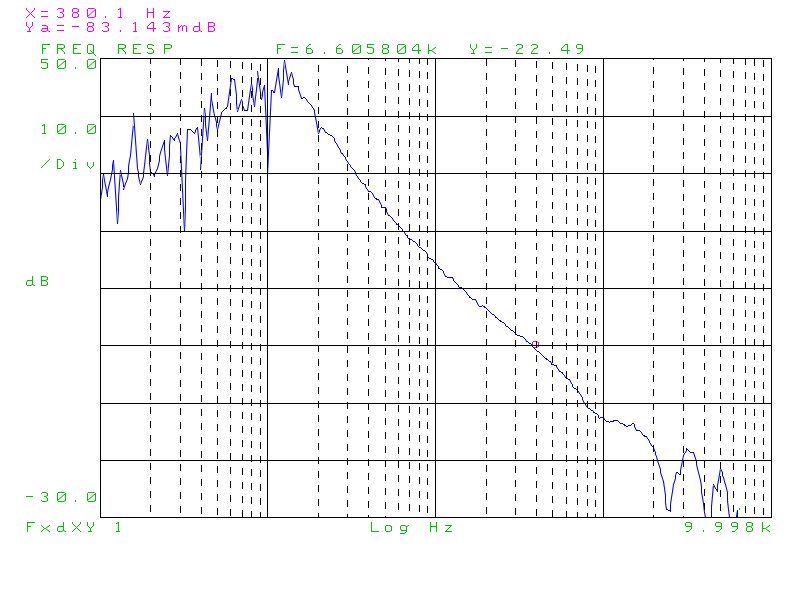
At each frequency, magnitude and phase response was collected, examples:
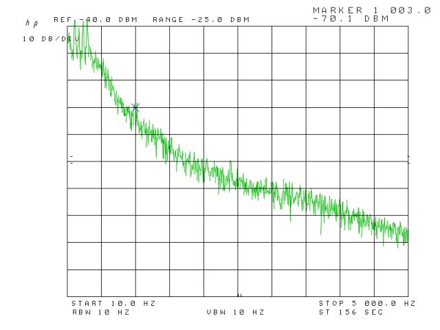
Gain (disregard the unstable response below 10 Hz, just an artifact)
mag_cp0

Phase
phase_cp0

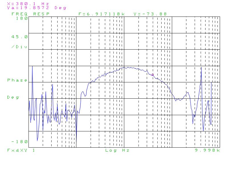
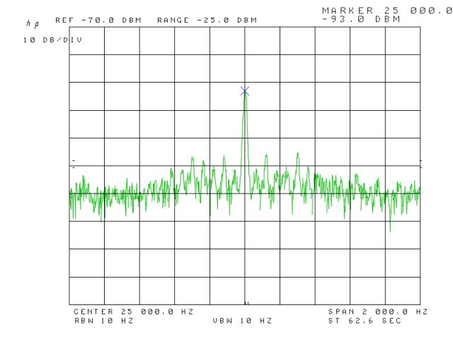
The interesting point is the 0 dB crossing of the gain trace – the unity gain bandwidth. This is determined for each test condition, and then the corresponding phase is obtained from the phase plot. In this example, BW_0dB is about 380 Hz, with about 20 degrees phase. Why is it so important? Simply because we need to keep this phase gap (of the A and B signals) well above 0 degrees, otherwise, the loop will become unstable-oscillate-massive phase noise of the generator will result.

Some call this the phase margin, so do I, although the whole discussion about gain and phase margins is typically centered around open-loop system, whereas we are dealing with a closed loop here. Fair enough.

Now, after some measurements, and number crunching, the results:

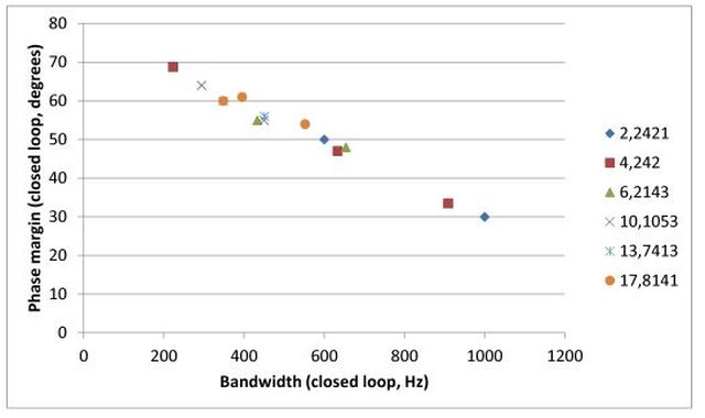
Phase vs. BW, at various frequencies
pm vs bw sg-811 pll
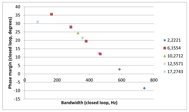
-you can see, the phase margin is virtually independent of frequency, and purely a function of bandwidth. So we can limit all further discussion to bandwidth, and don’t need to worry about phase margin separately. It is also clear from this diagram that we should better stay in the 250-300 Hz bandwidth region, for the given filter, to keep the phase margin above 25 degrees, which is a reasonable value.

Now, how to keep the bandwidth stable with all the frequencies and YIGs/SG-811 bands and sensitivities changing? Fortunately, the ADF41020 has a nice build-in function: the charge pump current can be set in 8 steps (0 to 7), from 0.625 to 5 mA (for a 5k1 reference resistor) – and setting the charge pump current (Icp) is not much else than changing the gain of the loop filter. The gain, in turn, will change the 0 dB bandwidth in a fairly linear fashion. Note: typically, the adjustable charge pump current is used to improve locking speed – at wider bandwidth, and mainly, for fixed-frequency applications – but is is also a very useful feature to keep bandwidth stable, for PLL circuits that need to cover a wide range of frequencies, like in the case of the SG-811.

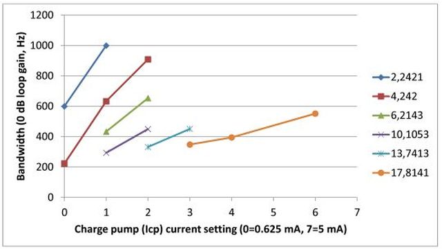
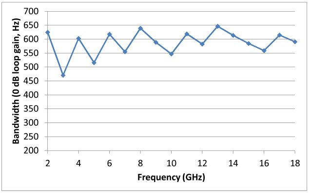
The next result – bandwidth vs. Icp setpoint
sg-811 pll bw vs charge pump current at various frequencies
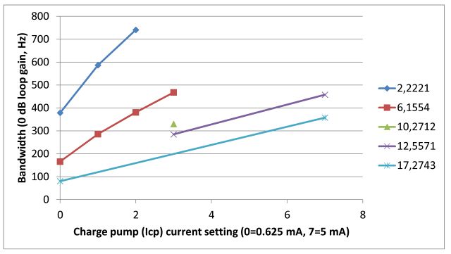
-looking at this diagram, the bandwidth is not only a function of Icp, but also a function of frequency. For the larger frequencies, the bandwidth is much lower. Some calculations, and it turns out that the product of bandwidth, multiplied with frequency to the power of 0.7 (a bit more than the squareroot) is a good parameter that gives an almost linear vs. Icp (see worksheet, if interested).
adf41020 pll bw phase margin

After all the measurements, things are now pretty clear – if we set the Icp current right, BW can be kept stable, over almost the full range, without any extra parts and switches, and about 300 Hz seems to be a reasonable compromise of PLL speed and stability.

Estimated PLL bandwidth (0 dB), using the Icp current adjustment of the ADF41020
bw vs frq with charge pump current adjustment
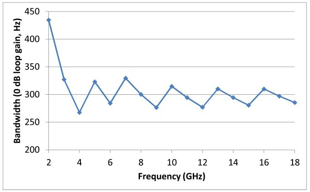
At the lowest frequencies (2 GHz range), the BW is found a bit larger than desired, but still, the loop still has 20 degrees margin.

Well, with all the phase margins and uncertainties, is the loop really stable enough? To check this out, what is typically done is to first try a few odd frequencies, at the start, end and in the middle of each band and monitor the VCO control voltage with a scope, for any oscillations or otherwise strange behavior. Then try a few small frequency steps, and see how the loop settles. This all went without any issues.

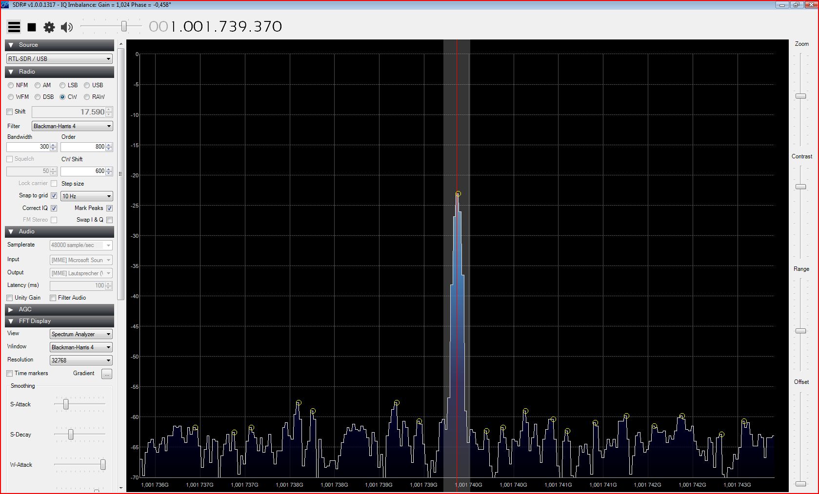
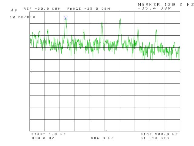
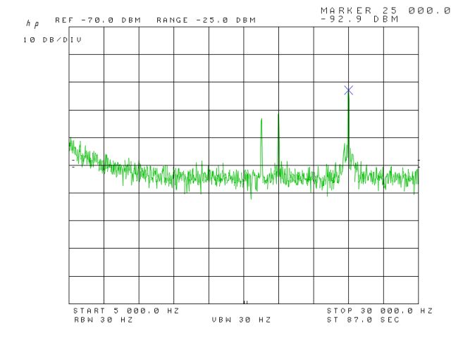
Still, to be sure, especially close to 2 GHz (increased bandwidth), a test was performed by injecting a 100 mV (nominal) squarewave, 10 Hz, via the test port mentioned above. The loop output spectra showed that this worked, and that the 10 Hz contribution is significant, while still not swamping everything else and driving the loop out of lock right away.

Power spectra with test signal on (upper diagram), and off (lower diagram).
pll power spectra

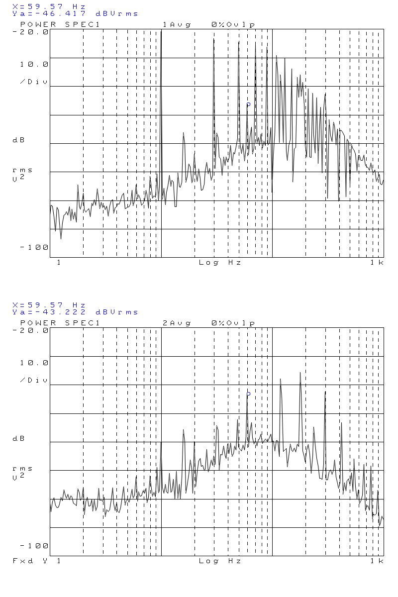
There are some 60 Hz/harmonic 60 Hz spurs, mainly due to coupling of 60 Hz to the coarse tune line, which is just a plain coax cable that doesn’t provide any good shielding vs. 60 Hz (or 50 Hz, in Europe) interference.

Needless to say, the PLL will not stop working right away when the phase hits 0 deg at the 0 dB point (see above, phase margin vs. bandwidth plot – even at negative phase, measurement was still possible – as long as the amplitude of the test signal is kept small).
There will be signs of instability, and this is what this test reveals. So the frequency was set again to 2.2221 GHz, and the charge pump current Icp increase step by step, from 0 to 5. At 6 and 7, no phase lock could be achieve – fully unstable loop.

Step response (AC component only, square wave, 10 Hz at nominal 100 mV, supplied to test port)
pll step response 2.2221 ghz 100 mV
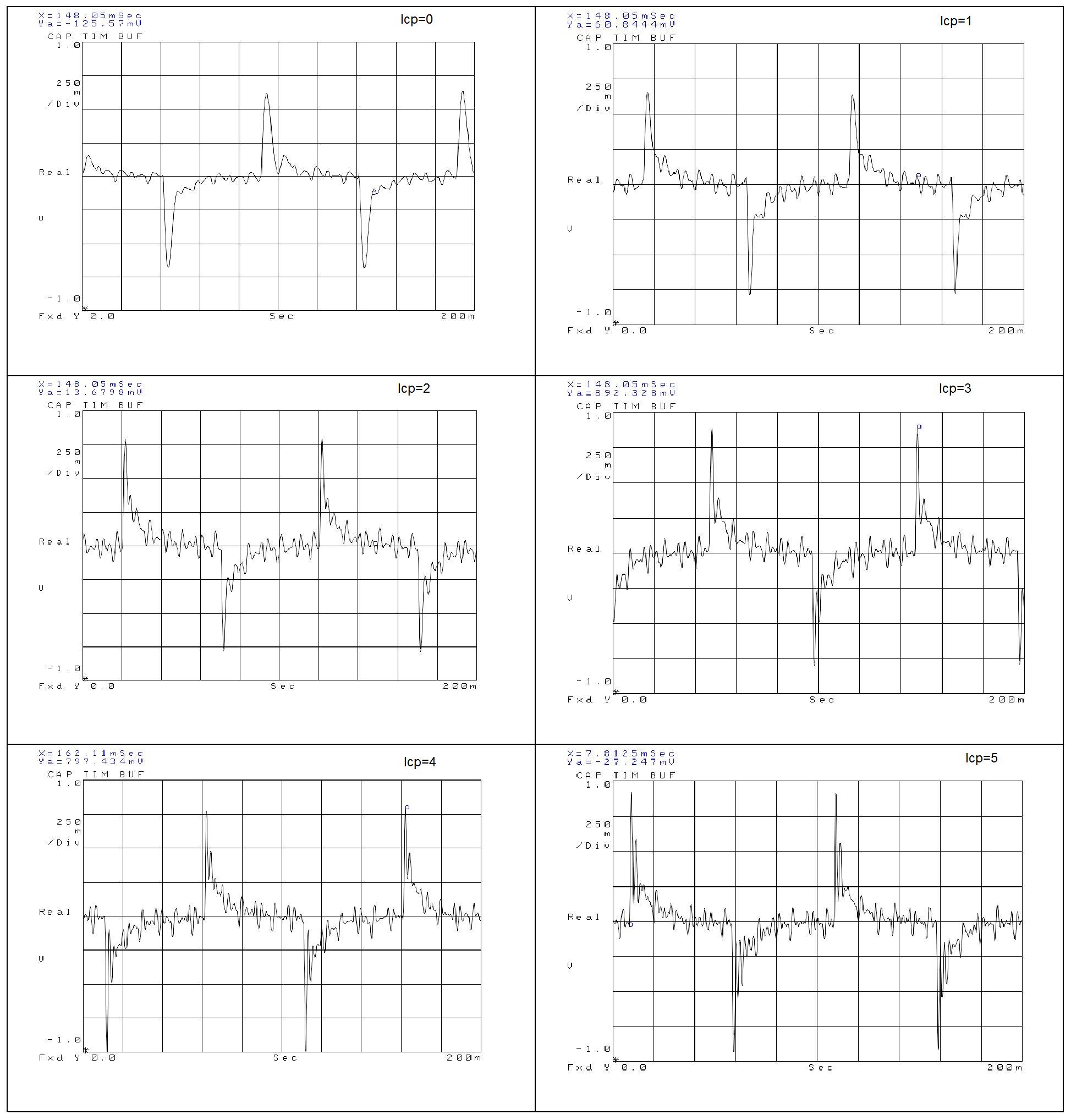
Icp=0 – this is the most stable condition, phase margin is about 20 degrees. Already at Icp=1, phase margin of about 3 degrees, stability is much compromised/considerably more noise, not only for the step response, but also during the steady portions. At Icp=2 and above, phase margin is negative, still, phase lock is robust (will not re-lock, once lock is lost), and the pulse response suggests to stay away from such regions.