Takeda TR6142 / Advantest R6142 Programmable DC Voltage/Current Generator: a busy CPU

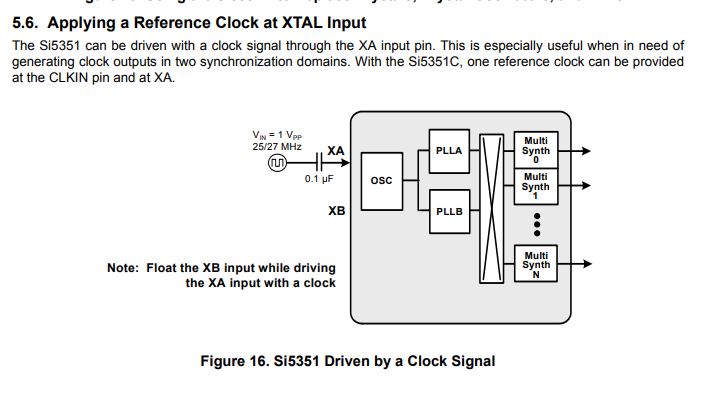
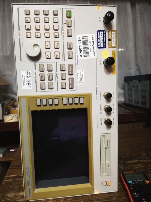
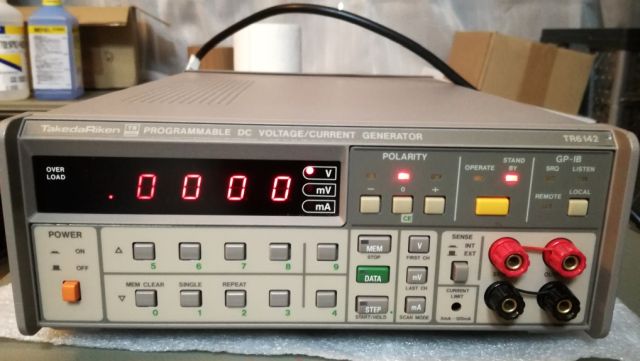
This is a Takeda TR6142 (also known as Advantest R6142) programmable DC source, a great find at less than EUR 50, of course, in non working condition.

The item arrived in good shape, but unfortunately, as described – non working, display comes up but no reaction to any key press. It just won’t interact with the operator.

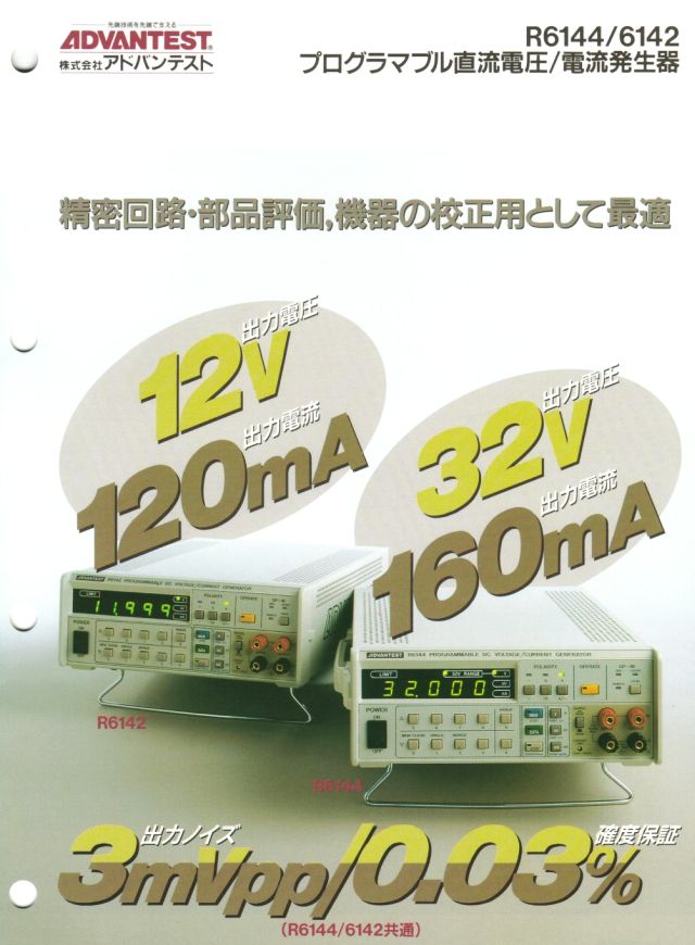
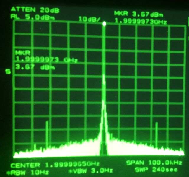
This 6142 is almost a cal standard type of source, 0.03% over 6 months (probably, for several years), 3 mV peak to peak noise, etc., it is also great to test semiconductors or to provide defined voltages and currents (up to 12 Volts, up to 120 mA), to devices under test, or circuits under development.

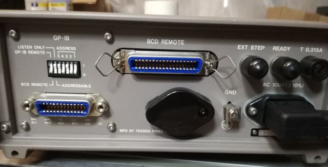
As an interface, there is a BCD input, and a IEEE-488 (GP-IB) input.

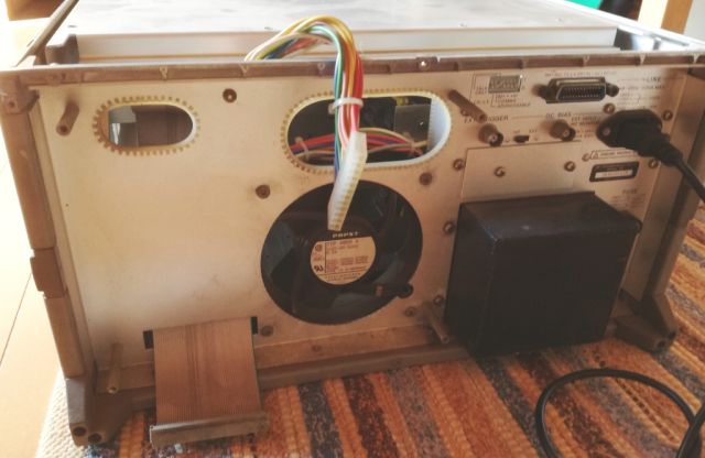
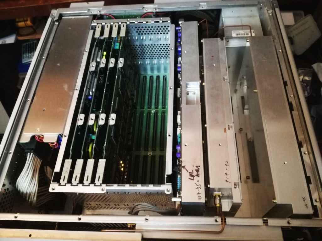
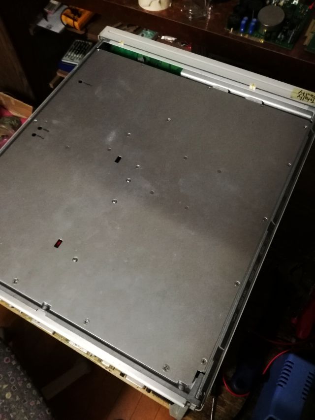
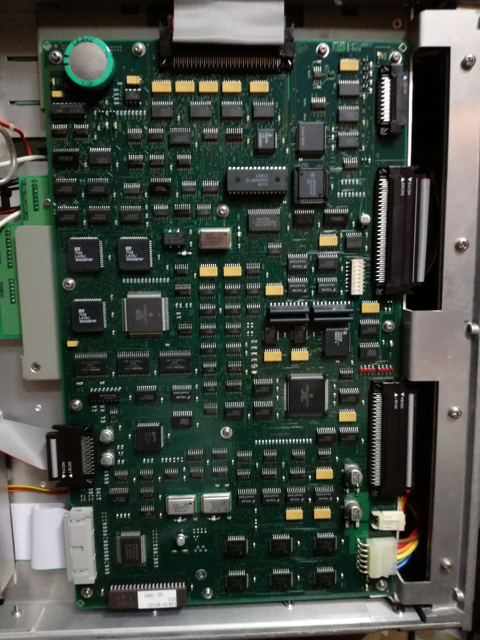
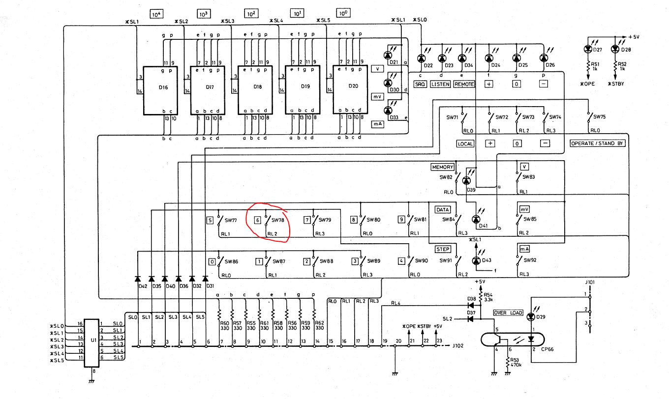
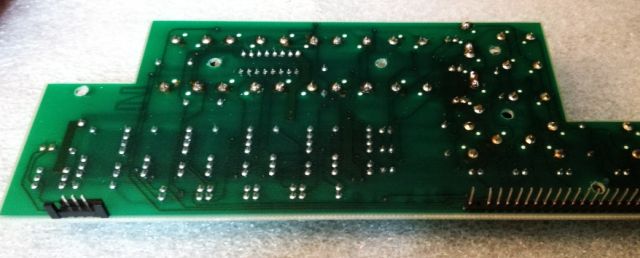
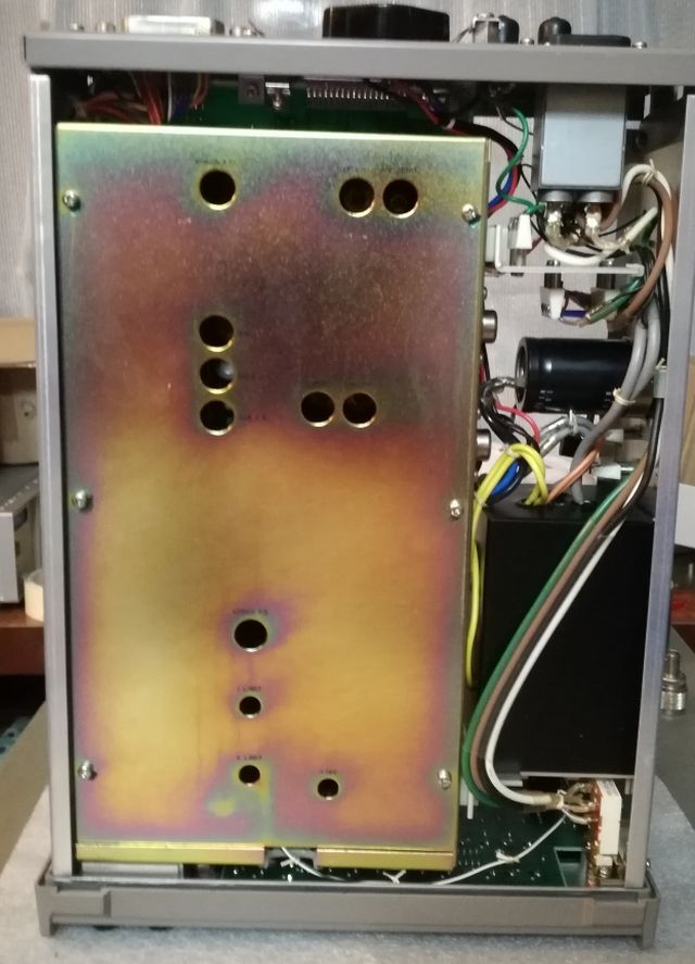
Looking inside, there is a logic board on the top side, and a shielded box with the analog circuits at the bottom. Fortunately, there is a manual with schematics available, let’s do some probing. Seems the CPU is waiting for something – it is not executing any commands, when I look at the data bus with a scope probe. What could it be? Checking all the inputs to the CPU – there are not many, mostly, the GP-IB, the BCD interface, and, the keyboard. The keyboard is a matrix design.

Turns out, one key is stuck! These buttons are some kind of pressure sensitive switch – they don’t have a “click” or other clear action when you push them. It could be just dirt or age that gives low resistance. Unfortunately, these switches are difficult to disassemble, so I soaked the switch in some isopropanol. Another thing that helps is to resolder the keys really hot, this will melt away the dirt layer (which may be just some organic residue or moisture) inside of the switch, and also cure any solder joint issues with the keys, although I didn’t find any – but the pins are somewhat oxidized.

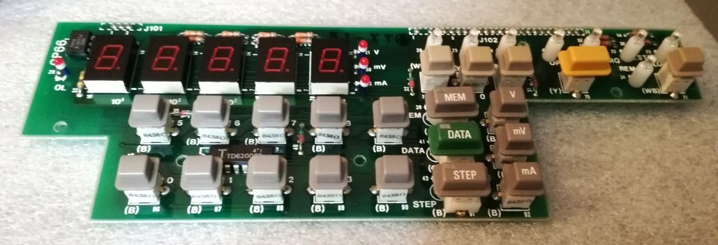
That’s they keyboard assembly, cleaned and resoldered.

After this fix – all is working fine, and the unit is responding to entries.

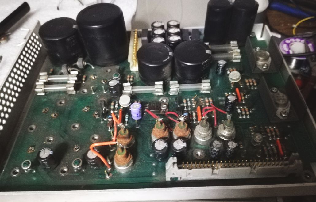
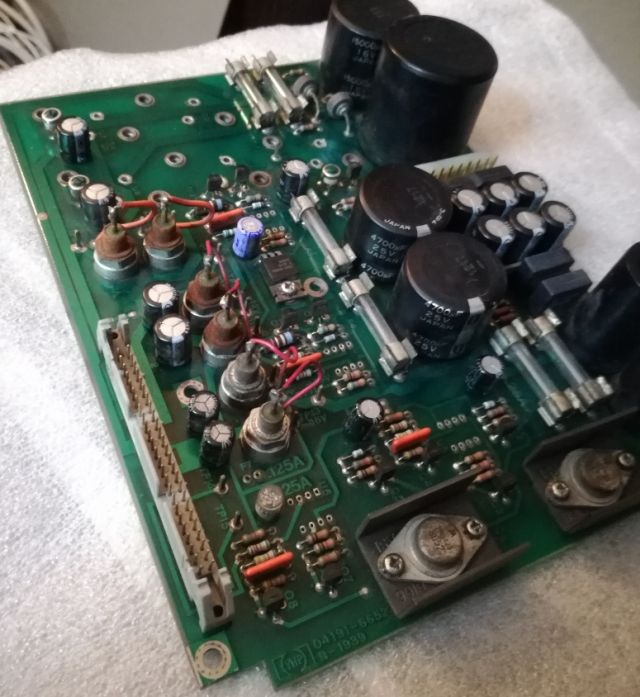
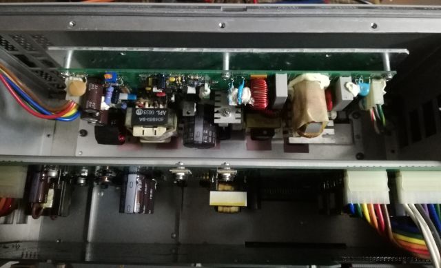
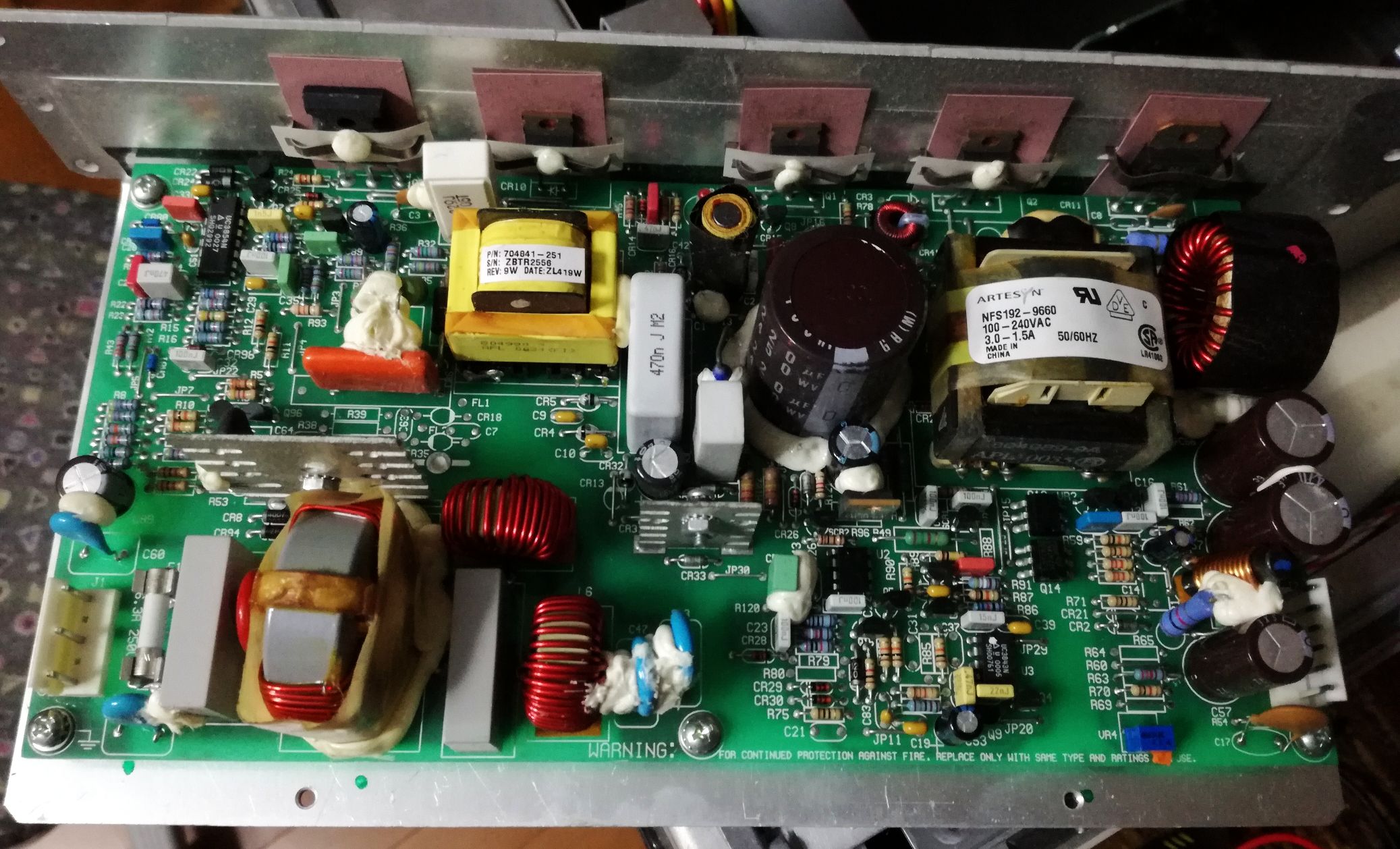
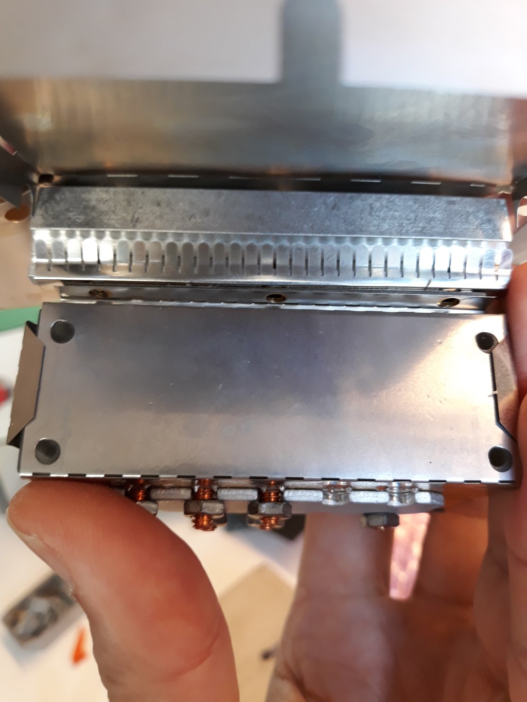
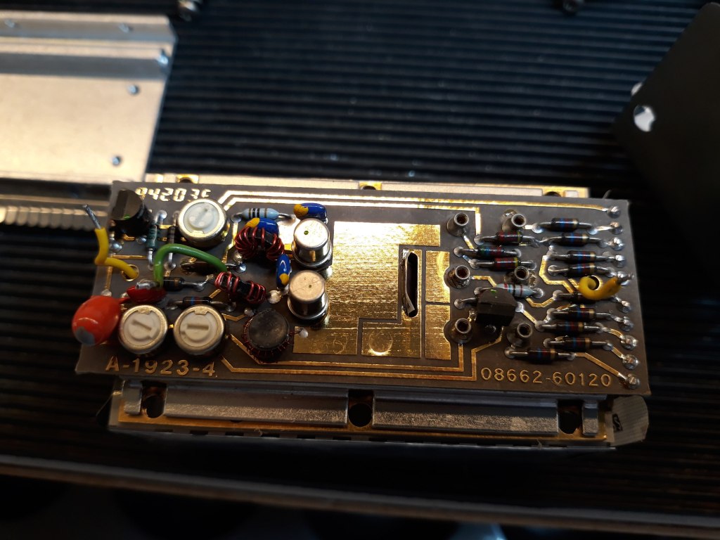
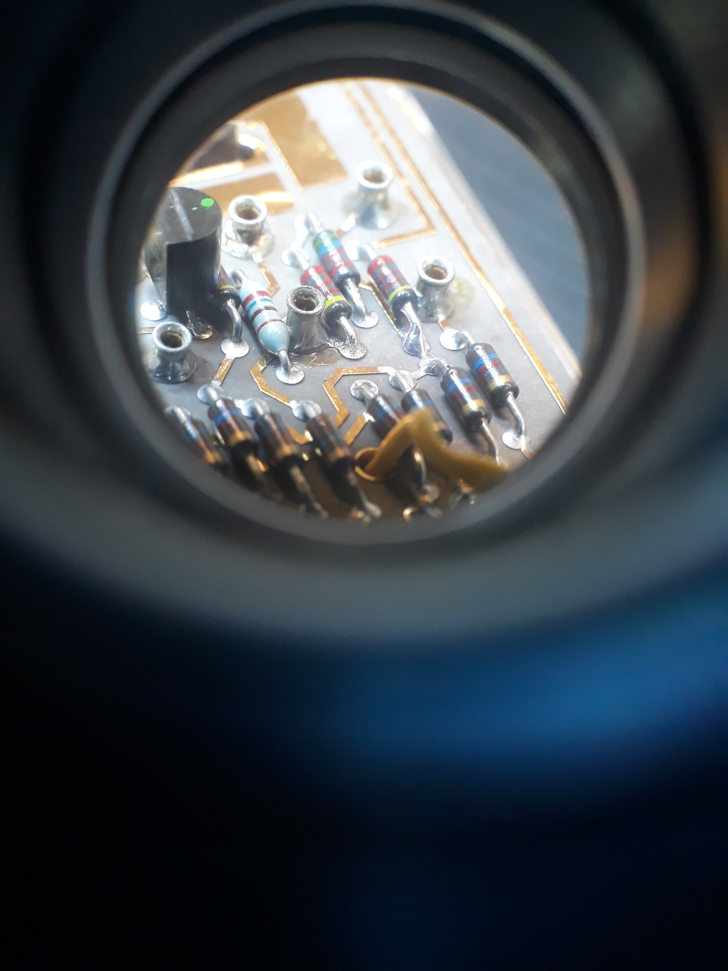
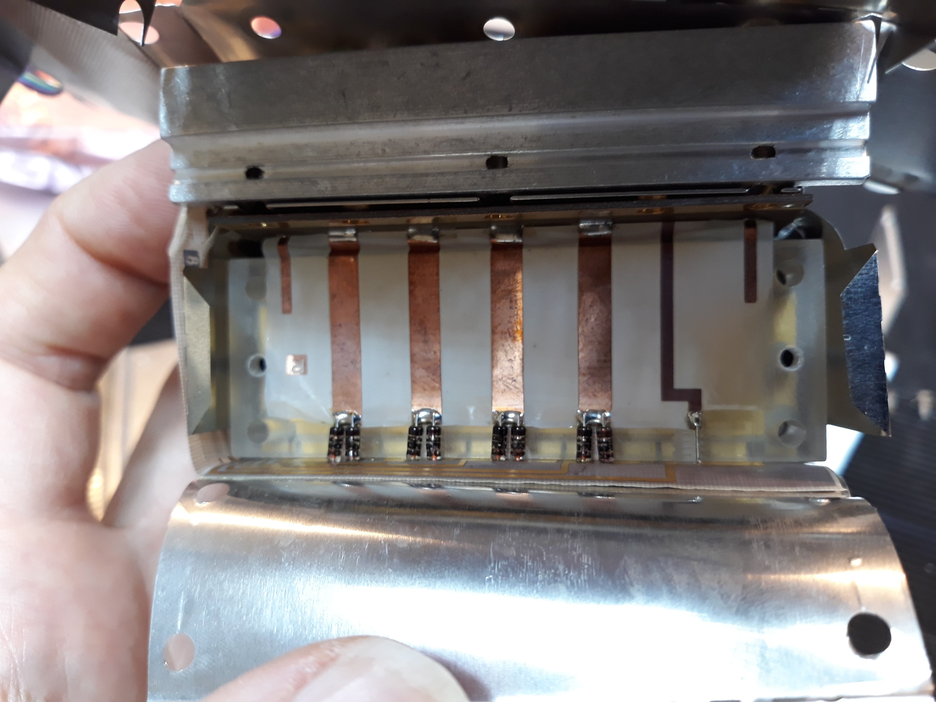
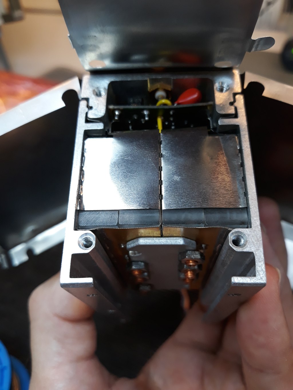
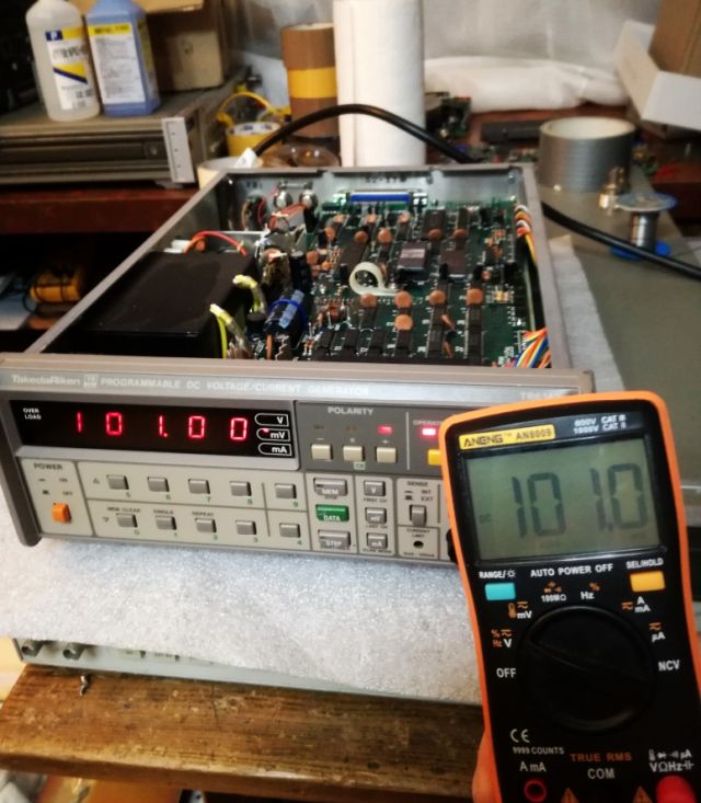
A quick look at the analog assembly (to check for dirt or other signs of aging) – no dirt found.

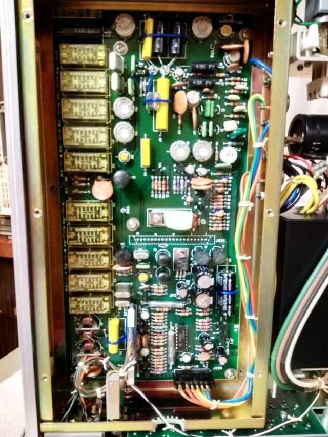
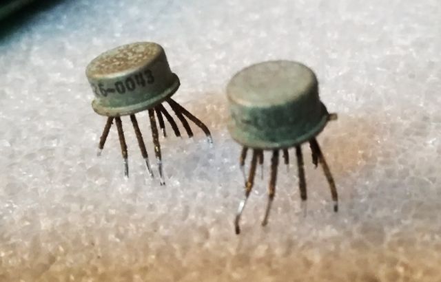
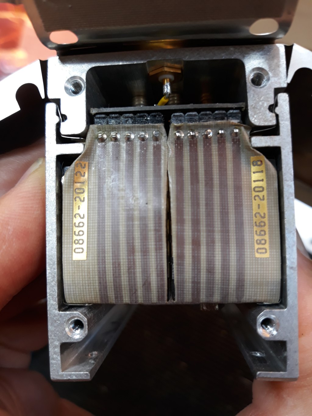
All is built with really high precision metal encapsulated resistors, teflon standoffs, and DC filtering.

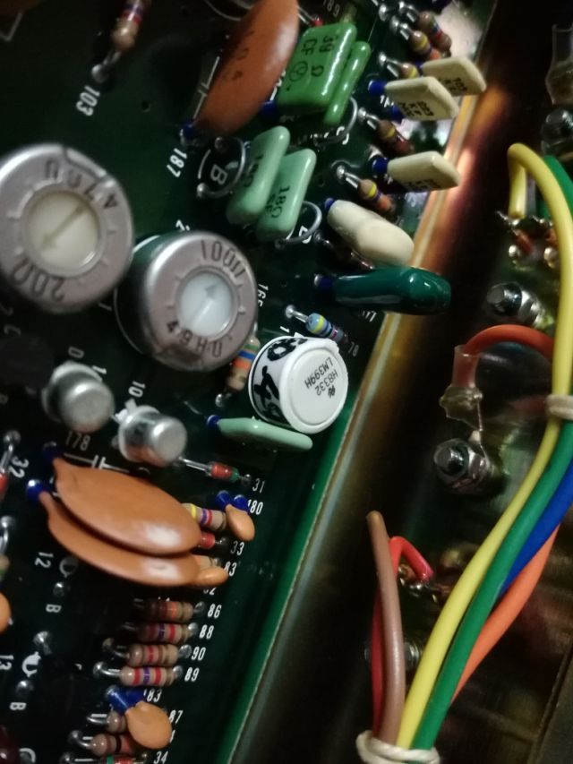
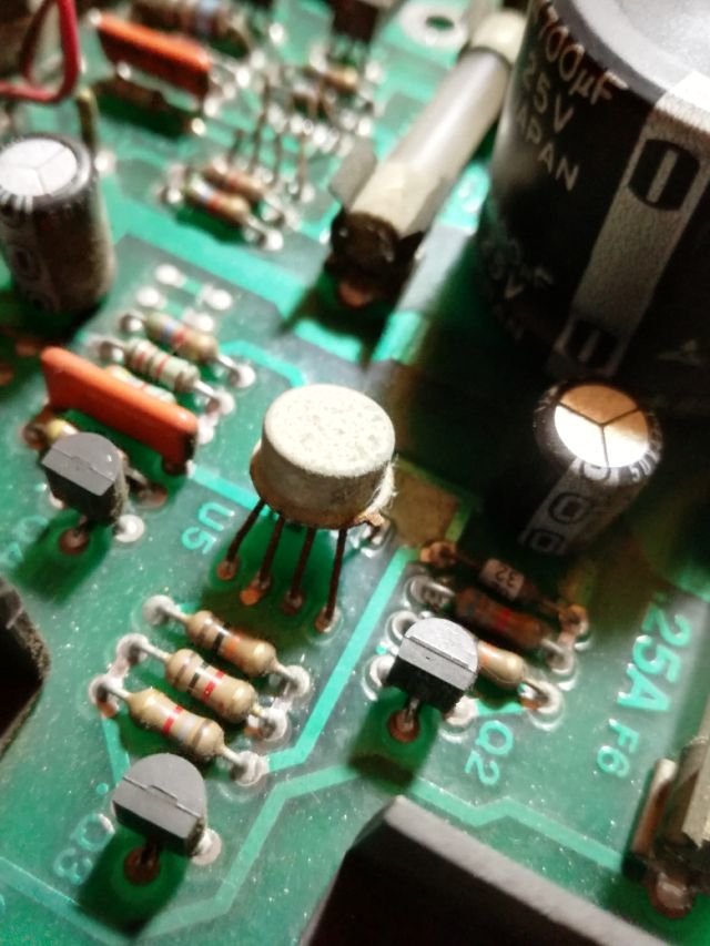
The main reference is a LM399, (0.5 ppm/K temperature coefficient, low noise, and, typically, 4 ppm drift per year).

A quick test – with a simple instrument – it is working just fine (also tested the current mode).

Now, another topic – I am currently working on this instrument in Japan, 100 VAC mains voltage, but later would like to operate it in Germany, 230 VAC.

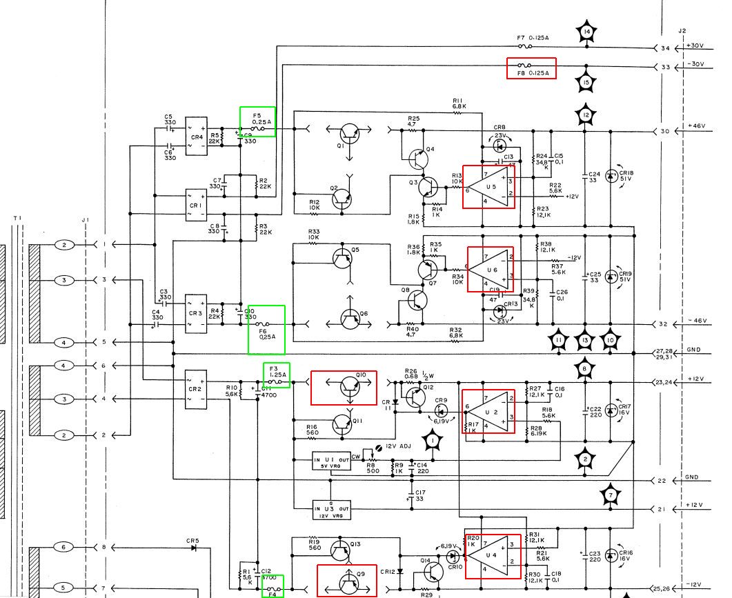
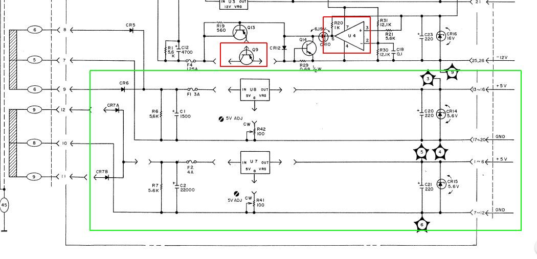
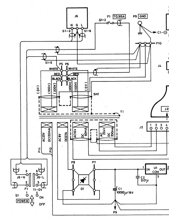
A quick look at the schematic – not good! There seem to be 100 V and 200 V coils on the transformer, but no provisions for 230 VAC! That’s not good.

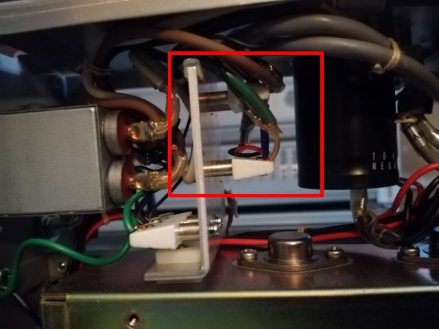
Let’s check the actual voltages and ratios – there is a solder terminal inside the unit.

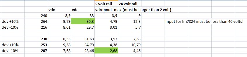
As it turns out, the schematic is either incorrect or outdated, the coils on the transformer are 0-100-120 VAC, and 0-100-120 VAC. So we can easily configure it for 220 or 240 VAC, yet, not for 230 VAC. The 6142 is rated for a +-10% mains voltage tolerance, same as the tolerance limit in Europe, for the 230 V (although it rarely deviates from 230 Volts by more than 2 Volts at my place in Germany, in the middle of a city with lots of industries and arm-thick power cable going into the building).

A calculation shows the ranges – it will definitely be better to configure it for 240 Volts, rather than 220 Volts, to avoid a dangerous over-voltage condition.

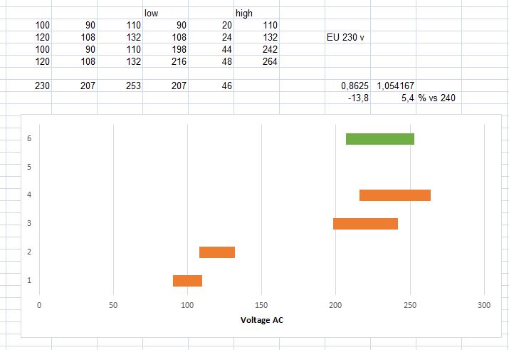
But what are calculations, if you can do measurements (with the unit loaded). Seems there is good margin in the DC voltage design, and the voltages regulators are standard 78xx types, with maximum 2 Volts dropout voltage – and with the voltages measured, even in case of 230 VAC-10%, we will still have a working unit, and stable DC rails. So, once back in Germany, we will just change the solder bridges in the voltage selector, and all will be ready for 230 VAC mains.

HP 8561E Spectrum Analyzer: 600 MHz troubles

Some investigations into the 600 MHz generation of the 8561E. The target is clear, we need to get a clean 0 dBm 600 MHz to the 2nd converter to make it work (the converter itself is running at 3600 MHz). The source, it is on the A15 board, which is one of the more complex circuits that have been designed by some clever engineers at HP. And, there are multiple versions of this board to make things a bit more complicated.

The 600 MHz system is located in the corner close to the J701 connector (which goes to the 2nd converter). It works by first locking a 100 MHz source to the 10 MHz reference, and then multiplying it to 300 MHz (which also drives other circuits, and the calibration output – which is working just fine), and then doubling it to 600 MHz followed by some amplification. Only output J701 is used, the other output, no use in the 8561E (and also this has low output).

The suspicious section, what could be wrong. Most suspicious, the output amp, because there is 600 MHz present, just not enough signal power. So this amp could be blown, and absorbing energy rather than adding RF energy.

It is a quite common amplifier, MSA-0386 which is a 12 dB silicon bipolar amp (labelled A-03 on the package). Ordered a few pieces, less than 1 EUR each, and these are useful parts anyway.

Other faults could relate to the input amplifier, but would we then get 600 MHz at all? The diodes – these are not likely to fail. The power supply decoupling – which has several capacitors and tantalums – may be faulty, but in general, the A15 boards don’t suffer from bad tantalums.

Well, first we need to get some small Torx bit, to get into this assembly…

HP 8561E Spectrum Analyzer, 30 Hz to 6.5 GHz: some consequences of a past disaster

Even today, 6.5 GHz bandwidth spectrum analyzers don’t come easy, you are looking at 6+ kEUR for even the most basic Rigol or similar low cost brand unit (which won’t be very useful to design VCOs or other precision gear), and all the high quality low SSB noise instrumentation, it is well outside the budget of the common hobbyist or even small company in this frequency range. This may be one of the reasons why the earlier HP and similar name brand equipment still is in high demand, and good working units still have their market, even being 30 years old. Some claim that with age, the performance might degrade, but as per my own tests and experience, this is not the case. These YTOs and YTFs and mixer still work like at the first day. Well, only if they work at all…

Here, we are dealing with a unit described as non-working, in good general condition, but not showing any signal, except, noise. The price was right, there doesn’t seem to be a big demand for defective spectrum analyzers in Japan – I was the only bidder.

Soon after the auction, a large box arrived, and the 8561E powered on just fine, with a good display (well, after some cleaning of the CRT and filter). Checked with the 300 MHz calibration signal – no response.
Further to check, it is quite handy to use a comb generator. This one has good output well into the high GHz range, at 100 MHz spacing.

The result – no response of the 8561E in the low band, and some minor response in the upper band (the 8561E uses 1st harmonic mixing, but two bands, one below 2.9 GHz utilizing a second converter, and one above 2.9 GHz, directly mixing down to 310.7 MHz first IF).

That’s how the comb gen output should look like on the analyzer (below, tests with a different – working – analyzer): all equi-desitant peaks, 100 MHz spaced, and somewhere between -10 and 0 dBm.

Next, I checked the LO, and it is osciallating and it is phase locked, and the power level is right, at least at the LO output. That’s a relieve – at least the YTO is working and locked, and no complicated PLL troubleshooting.

Well, what can we do further, we need to take the thing apart (at least, I have the manuals and even the component level information package, CLIP), starting to probe the signal chain. The most easily accessible part is the mixer (all bias/switch voltages checked OK), let’s take it out and see if it works – feeding a test signal directly to the mixer, and taking the output to a working analyzer.

Low band – looks fine.

High band – working, but we are missing 25 dB signal strength! Something is not right.

Let’s have a look inside – nothing obvious like a broken bond wire, or burn mark found – but also hard to find without a microscope.

Reparing the mixer itself, no option here, this a marvel of engineering, and you need a larger workshop than mine to fix all these tiny pieces of silicon, mounted with gold on axis-oriented saphire substrate…

This may become a more serious repair, over several weeks to get spare parts in, so best to keep all parts and screws well arranged, I keep them in plastic bags, so I can check later if all made it back to the instrument.

Now, with the mixer situation clear – it has a defect in the high band, lets turn to the incomming path, from the main connector, to the mixer input.
Low band is fine, but high band again – weak signal. What can we do? We can at least isolate the fault. Turns out, the attenuator is working just fine, but trouble with the SYTF. HP introduced this combination of a solid state switch and a filter with 8561E, the 8561B still had a separate switch (which would be easier to fix, compared to a fancy switch-YTF combination.

Next, let’s check the IF processing path – just feeding a 310.7 MHz signal to the analyzer, past the mixer and 2nd converter – all working fine. Great!

Next, let’s check the 2nd converter that is needed for the low band using a 3.9107 GHz 1st IF. It is not converting, and no 3.6 GHz signal at the test port (the LO of the 2nd converter is generated by multiplication of a 600 MHz signal). Further check shows that the 600 MHz signal is low, about -20 dBm (should be about 0 dBm). Still the 600 MHz is phase locked, and the reference output (300 MHz, but derived from the same circuit), is working, so probably something with the 600 MHz output stage.

Let’s review. (1) a dead mixer, (2) a dead SYTF, (3) a probably working 2nd converter (at least as much as I can tell now, with feeding a good 600 MHz signal), (4) working LO system, (5) working IF and other processing system, (6) good CRT and mechanical structure. And, looking at the noise specifications, and the total package of properties – is it worth the repair? Well, used units in mixed state go for 2 kEUR, good calibrated working units for 4-5 kEUR, so if we can find the spare parts (a mixer and a SYTF) for a few hundert EUR, it will still be a very economically reasonable repair. Fortunately, I was able to locate a “working and guaranteed” mixer, and a spare 2nd converter (just in case) for a good price. Only the SYTF, a bit more expensive, but it is guaranteed working as well. Now, we need to wait for these parts to ship from the US and China, to Japan.

I wonder what has happend in the past, what kind of disaster? Usually, the mixer is not easily damaged, because of the limiting characteristics of the YTF. And the 600 MHz fail looks completely unrelated. But who knows the sequence of failure, maybe the 600 MHz failed long ago, and the analyzer was only used in the high bad, well, until someone connected it to a high voltage generator.

A few other things to consider – the lithium battery. It is still good. Usually I only change them once defective, or in case I sell an instrument.

The fan, a Papst Multifan 8312 (working, but a bit noisy) is still available, but I will only replace it after fixing all the RF chain.

Another bonus – the 8561E also came with a working mass memory module. Mass refers to a massive 250 kilobytes in this context!

HP 4191A Impedance Analyzer: 1-1000 MHz

Recently, I found a defective HP 4191A for a low price, and thought I should try to fix it – these devices where manufactured by HP’s Japan division, and for years, I have been looking for a working unit, but to no avail (prices in the range of 2-4 kEUR, and new instruments of this class demanding well over 10 kEUR). So, let’s see if we can fix this box.

This is how it should look like, from the cover of the HP Journal.

This is the unit currently, already opened it up to have a look inside.

Top view – a good amount of empty space, which is there to fit the high frequency resolution option.

The CPU boards, it seems to be the newer version, compared to the boards described in the service manual.

Rear view – this also carries the power supply (voltage regular A23 assy). Already removed it, it was only held on by two screws. As it turns out, it is not working, the 12 V rails are missing. And some other voltages are not good (5 V is fine, so the CPU is working and seems undamaged).

The unit is reasonably clean, but the power supply, it is dirty, and rusted. Not sure why.

Especially the opamps have signs of corrosion – two had even non-conductive, fully rusted legs. These are 1826-0043, which is a pretty generic HP part and can be replace by LM307H (or the DIP version, much lower cost, LM307N).

I have never seen such rusted opamps, maybe the instrument (or at least this assembly – the rest of circuits has no sign of rust) was kept close to the ocean, in salt spray?

After more careful analysis, some trouble with the 12 V (positive and negative) pass transistors.

Seems someone tried to repair it before, but for some reason, judging by the date codes, didn’t replace them.

The NPN, no problem, it can be replaced by a 2N3055. But the PNP – it is HP 1853-0252, alias SJ1798. Not sure how to get one of these.

With some further analysis of the maximum current, and other parts of the circuit, I believe we can safely replace it by a very common and low cost MJ2955. This is the complementary TO-3 transistor to the famous 2N3055, and by all I can tell, it should work just find in this power supply, as a simple pass transistor.

In the meantime, the board has been soaked in some isopropanol, and brushed with a soft brush, and all the rusted opamps removed. Ready for the new parts to be soldered in, once they arrive.

Another thing to look at – the NiCd batteries aren’t good any more. These will be removed or replaced, once the other parts are working, mainly to avoid any future risk of leakage of these cells, messing up the instrument.

Anritsu MG3681A Digital Modulation Signal Generator: a digital box

Along my search for used&broken&cheap test equipment in Japan I came across a Anritsu MG3681A 3 GHz generator, it has quite impressive specs, and the unit offered had the full CDMA-W digital package, allowing a whole lot of experiments with digital modulation. The price was right (just about EUR 100 plus shipping!), so this was soon to become the the first Anritsu gear in my workshop.

The information from the seller – at least it powers on, and frequency is locked. The unit also has the Option 02 OCXO, a really high quality 10 MHz source, so even if all the machine is defective and broken, there is still good use for it, just using the parts for other projects.

Further tests confirmed that the output is low, albeit, it is locked and even the ALC (level control) appears to be working.

Without having a good insight into the workings of this unit, also because of lacking schematics and details, I decided to do some tests. After removing about 100 screws or more (the unit has double and tripple shielding to avoid RF leakage), I got access to the attenuator and signals going to the attenuator (see block diagram). Obviously, something is wrong with either the attenuator (a burned segment or reverse power protection element introducing loss?) or the detector, or the ALC circuit itself.

Checking the diagnostic messages – the MG3681A thinks all is good! The only strange thing is that I don’t get any ALC error message (unleveled message, even when dialing in +17 dBm output, which corresponds to about 12 dBm output at present).

A through check of the attenuator shows that it is working in 1 dB steps – i.e., the MG3561A is only using a 1 dB for linear adjustment of power, and all the other attenuation is by the switched/mechanical attenuator. This true up to +5 dB, above 5 dB, the attenuator is set to 0 dB and the gain of the output amp is determining the power. Same below -135 dBm. Attached detail from the service manual shows the detail.

After all, I was able to confirm good working condition of the attenuator.

Next, some tests of the output level of the RF amp assy, which feeds the attenuator. And, not surprisingly, the output power is already low before entering the attenuator. All is leveled and working as it should, and also flat regulation with frequency (!), but too low power.

Following the service manual, there is a complicated procedure for output power adjustment. It requires some special software, and two more Advantek instruments that are hard to come buy, and actually, we don’t have any issue with flatness or response, but just an offset of the level. So we should be able to correct this somewhere in the analog circuit, say, in the opamp doing the ALC control, or in the DAC setting the output level.

Studying the circuit a bit, with the block diagram, and some general knowledge about such analyzer. The function blocks are clear. And a quick test showed that the level detector itself is working. So we need to troubleshoot the level control loop and opamp. Another interesting observation – the digital control of the final amp is actually done by light beams (IR diode sending, IR receiver), to transmit digital information noise-free to the final amplifier. Note the gaps in the cover, marked in the yellow circle. That’s where the light passes from the digital control to the amplifier section.

This level control circuitry is part of the modulation assembly, which is a fairly complex assembly. But, what is this? There are several micro-size adjustment pots. Could it be that one of the relates to the ALC loop? How can we find out? Easy enough, we monitor the output with a power meter, and turn each of the pots a bit, of course, not without clearly noting its original position. The 3rd adjustment pot – it does affect the output power! And, surprisingly, I can easily increase the power by about 6 dB.

With this adjustment identified (I could not find any reference in the service manual to these adjustments), I rechecked and readjusted it output power at a range of frequencies from 1 MHz, 10 MHz up to 3 GHz, and flatness is in fact very good! Also, I get the expected performance now when increasing the output power past about +14 dBm – an uncal-unleveled message is coming up, indicating that the maximum output power has been reached (the MG3681A can provide about 14-15 dBm leveled power over the full range).

A good amount of logic in programmable devices (firmware of MG3681A can be updated, if you have any such firmware, please share with we!).

Another view of the inside of the instrument – it is what I call the Japanese test equipment design, a lot of empty space, all well arranged, and many different types of assemblies and hardware with great attention to detail and sophistication, and some manual corrections with superfine wire. Because of such design, it also needs two fans – one for the power supply, and one for the main unit.

The CDMA-W functionality. Fully working at least as much as I can tell from spectral analysis of the digitally modulated signal.

Some study of the phase noise performance. The MG3681 is not too bad, it has fairly low SSB noise, even close to the carrier.

For comparison, the phase noise of a 8642B, which is a good HP generator, not the best for close in phase noise, but it is a low noise and heavy and sophisticated machine, even without any digital modulation.

No sophisticated phase noise test gear set up here, but let’s study it on a 8561B analyzer, at 2 GHz frequency. At 100 kHz span, the noise of the analyzer dominates, and both the 8642B and MG3681A show very much the same levels.

MG3681A:

HP8642B:

Close in, at 10 kHz, the MG3681A appears superior, maybe, by about 10 dB. Not bad!

MG3681A:

HP8642B:

With all the functions established again – some clean up: removed all the dust, checked all the connectors, and put the thing back together.

Now, all is hidden again under several sheets of metals, and all the many screws (not only many pieces, but also many kinds) back in. Let’s hope we don’t need to open it soon again!

Some useful documents:

Anritsu MG3681A Technical Description

Anritsu MG3681A Service Manual

Anritsu MG3681A Datasheet

Si5351A + u-blox M7: Clock generator tests

With the Si5351A mastered, time for some tests with the actual application, the GPS receiver (and later GPSDO system).

Two tests were performed:

(1) Using the Si5351A clock generator with a standard, not specifically selected or particularly stable crystal. Presumably, an AT cut crystal, running at 25 MHz.

(2) With the Si5351A driven by a OCXO (HP 10811A, part of a 8662A unit – will be later replaced by a stand-alone unit using a HP 10811A with power supply and distribution amplifier, but essentially, to the same effect).

The first test, we need to set the registers of the Si5351A (check the Silicon Labs AN 618 Application Note – check it in a quiet hour, because it has a lot of heavy content…). 25 MHz clock input, 26 MHz OSC0 output – can be achieved by running the VCO at 650 MHz, and integer-only dividers.

For the calculation, I use a self-made Excel sheet, which allows me to play around with the numbers to figure out the best combination of dividers and VCO frequency.

Here, the over test setup:

That’s the Xtal used – it came with the board, and I couldn’t find any data on it. Appears to be an AT cut crystal. Starting from room temperature, frequency, will go down with increasing temperature, and up with colder temperatures.

Such temperature variation is easily introduced here in Japan. First, keeping the room at 22 degC by the aircon (A/C) unit, then switching it off overnight (cooling the room by a few degrees, maybe down to 17 degC), then, next morning, heating up again to 22 degC (and a bit more as we had a sunny day).

The detail below also shows the small thermal mass of the Si5351A, free-hanging in air. Better to enclose it or to add some thermal mass later, to avoid thermal-gradient introduced noise or instability. You can clearly see the on-off cycles of the A/C unit regulating the room temperature.

After all this study, we find out that we can use the GPS and Xtal as a quarz thermometer (such thermometers really exist!)!

Test 2, now running with a 10 MHz reference clock, and still 26 MHz output to the u-blox M7 (in all cases, the u-Blox has been modified by removing the TCXO, and feeding the clock signal directly to the GPS chip). Sure I known that I am running the Si5351A outside of the specified range – but after all the research, Si5351A Spec, Myth and Truth, I believe this is OK.

The test setup – note the dotted additions – this will be the later phase locked circuit.

The register settings – running the Si5351A VCO at 780 MHz allows the use of integer-only dividers.
Capacitance set to 4 pF (the lowest value possible for the Si5351A, but it has little effect on sensitivity, 10 pF default setting works as well, maybe 1 dB decreased sensitivity, but we are anyway feeding more then enough power to the Xtal A input of the Si5351A).

The GPS clock drift data – not very exiting – no drift at all, less than 1 ppb over a few hours. There is a slight frequency offset, because the electronic frequency control (EFC) of the 10811A OCXO set to 0 Volt, rather to the proper value for exactly 10 MHz, only for convenience and to avoid any artifacts from EFC DAC noise or drift.

The position accuracy also seems better with the stable oscillator, but may need to check this again after acquiring data for a full day or so.

All in all, more than a proof of concept. Next steps include setting up a stand-alone OCXO (I have a couple of spare 10811A OCXOs around), a distribution amplifier (nothing special, planning to use some 74HC14 with small signal transformers for isolation), and getting the PLL code into a microcontroller. For the DAC, I will use a fairly basic model, and provide a low pass filter at the output (much faster than the digitally-generated long time constant low pass of the PLL loop, but still slow compared to common standards) to reduce noise.

So far, the bill of material is very low, just a few dollars, including the GPS receiver. My goal is to stay below USD 10 total, excluding the OCXO, to achieve better than 10-9 stability, and an output with no jitter or other issues.

Si5351A “Any-Frequency CMOS Clock Generator and VCO”: Specifications, Myths, and Truth

The Si5351 series of silicon-VCOs and clock generators is a quite remarkable achievement of technology. Earlier on, we needed two sets of dividers, PLL control logic, and a VCO – essentially a box full of parts – to realize the same purpose: generating one clock, from another.

While being quite adaptable to all kinds of circumstances and uses, the Si5351A (which is the cheapest, and most common chip – all the others have so many pins, and are in such small package that they are hard to use) has some limitations.

(1) It only has a crystal (XTAL) input, specified over a narrow frequency range. 25 to 27 MHz. Some forum comments suggest that there is a tuned oscillator inside, only working at such frequency, Myth or Truth? For my particular application, I need to drive it by a 10 MHz external clock, because that’s the main frequency source and signal I have available.

(2) The VCO range, 600 to 900 MHz should be selected, according to the instructions. Any chance to use lower frequencies, in case this is needed to get integer-only division ratios? Or higher frequencies? What are the limits?

To test the Si5351A, we can use one of the cheap break-out boards. I used the CJMCU-5351. Including SMA connectors, just a few bucks! I can’t really make it any cheaper, and this board also has level translators, and a 3.3 V supply, which is needed because the digital control will be running on good old 5 Volt logic. The I2C control signals are conveniently provided by a Atmel Atmega168PA controller, from a shared 5 Volt I2C bus.

Some modification is necessary – we need to remove the crystal, and add a small SMD capacitor, and a short wire. Once of the outputs, we cut the trace an re-purpose it as an input.

Before modification:

After modification:

The schematic, it is quite similar to the connection method suggested in the Si5351 datasheet.

Datasheet:

Actual modification and test circuit:

Obviously, to test the Si5351 over a range of reference input, we need to set the internal dividers (to lock the VCO to the reference clock input, and to divide it down to a suitable output frequency) to suitable values. Generally, 900 MHz VCO frequency, and 0.5 MHz output frequency has been selected. The low output frequency helps to see any glitches and jitter on my rather moderate scope I am using here (a 60 MHz Tektronix analog scope). At each setting, I increased the reference frequency until the Si5351 lost phase lock. Also, I reduced the power level at each frequency until some jitter showed up in the output.

The tests took more setting than expected – because the Si5351 can handle a huge range of reference frequencies – well beyond the 25 to 27 MHz, and even the internal divider can be set outside of the specified range (necessary only for the highest reference clock frequencies). A particular useful fact – the Si5351A can accept input frequencies of 100 MHz easily – I have some microwave PLLs running of a 100 MHz (rather than 10 MHz) reference.

As you can see, the internal VCO is working from about 170 to about 1100 MHz, so the 600-900 MHz is a good suggestion, but you can also run the VCO at, say, 500 or 550 MHz, if needed in some specific case of division factors (it is always much better to use integer-only divisors, rather than any fractional terms which introduce jitter and spurious signals.

After all this study, we can also plot the input sensitivity (signal from a 50 Ohm source, directly AC coupled to the XTAL A input, XTAL B floating, no other termination – probably, I will measure the characteristic impedance of the input later, no suitable test equipment currently available here in my temporary Japanese workshop).

As you can, see there is no tuned circuit or anything like it, the xtal input can accept any signal up to the highest relevant frequencies, and at lower frequencies, you just have to drive it a bit harder. 10 MHz may be the useful low limit (I suggest you drive it at 3-5 dBm when using 10 MHz, which will be about 6 dB above the sensitivity threshold).

Now, up for some long term test in the actual GPSDO application!

Agilent 4352B VCO/PLL Signal Analyzer: a great find (hopefully!)

I found a great deal on a “totally faulty” 4352B, well, it is a bit a cat in a sack, as we say in Germany, you never know what you get. It shipped from Manila, even better! List price, I think it was close to USD 50k!

It’s a clean unit, except for about 100 stickers and seals!

All heavily shielded, many kinds of screws and metal plates to keep to good waves in, and the bad waves out.

The brain of the machine – quite sophisticated – Japanese engineering (this unit has been manufactured by HP Japan!).

After some study and test, it is clear, it is dead because there just isn’t any power. The power supply is a two-stage supply, first stage, a switchmode universal voltage to 24 Volt (190 Watt) supply, bz maker Artesyn, then a really top quality 2nd stage, made by Agilent. And guess what, the 24 Volt supply is faultly!

This supply uses power factor correction, and two IRFBE30 MOSFETs to drive the transformer – one of them is shorted shot. Otherwise, no damage to be found on the board so far, except the thermal fuse, which must have cut out immediately (even the primary fuse is OK – so there is hope that this will be an easy repair of the 24 V supply).

Ordered some spare thermal fuses and MOSFETs, quite common IRFBE30 type – low cost. Let’s see if this will let us get the power back, if not, worst case, we can always install a new 24 V 200 W supply – there is enough space in the case.

In any case, these VCO analyzers are a great deal – there is a 26.5 GHz (!! APC 3.5 !!) power splitter inside, value, still available today, EUR 1350, and a 13 GHz detector, value, 450 EUR. But let’s keep fingers crossed that this won’t become a parts unit anytime soon.

The 08662-60001 low noise VCO: the heart of the HP 8662A

This is certainly one of the electronic antiques and marvels, which had the most hidden and non-spectacular impact on mankind and development of mobile communications in the 80s and 90s – the VCO of the 8662A/8663A, the defacto standard for low close-in phase noise signal generators.

The concept, it is a switch reactance oscillator, i.e., the inductances will be switched, to cover the 320 to 640 MHz range, rather than doing this all by varactor diode tuning.

For low phase noise, you need an oscillator with high Q – this is achieved by strongly biasing the varactor diode over the full tuning range, and by low resistance PIN diodes (two in parallel, see below!), that switch the thin-film inductances embedded between lexane disks.

Note the small indent on the golden patch on the PCB? This is where the copper bolt reaches in to adjust the frequency offset.

All this is housed in extruded aluminum, end a layer of special steel which absorbs magnetic fields. So far, I never had the chance to look inside of these – but a kind reader this block, Martin, shared this picture and I put it up here for those interested.

The designer of this marvelous and magic device, his name, Dieter Scherer, a German fellow of HP, unfortunately, I have never met him and don’t know if he is still alive. Sure he left behind great achievement and a legacy of high frequency engineering.