Micro-Tel MSR-904A Microwave Receiver: three bad guys, an a revised YIG filter

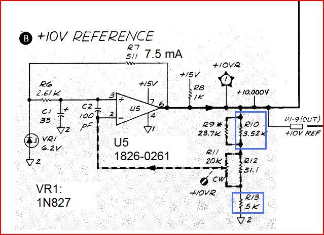
There are a few remaining items that need to be fixed:

(1) The frequency marker doesn’t work
(2) The AGC circuit is acting up a bit
(3) The 21.4 MHz IF chain – it is working but gain seems low
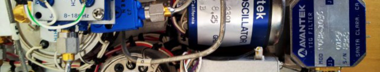
(4) The YIG driver – it has too much inherent noise when using the external input (EXT frequency mode). Added a 100 n capacitor (see earlier post) – but this interfers very much with the faster sweep rates, where full YIG driver bandwidth is needed. So I need to add a switch that takes out the 100 n cap, except when in EXT mode (not planning on any super fast sweeps in EXT mode, but definitely need low phase noise)
(5) The ‘signal strength indicator’ is working (a nice LED bargraph), but the offset can’t be adjusted properly, and it moves eratically, at times.

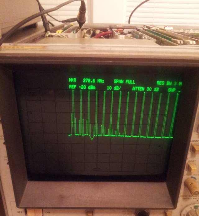
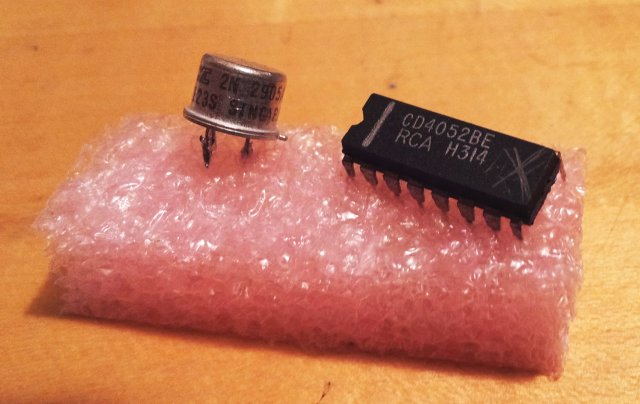
With the manual, the search defect (1) – marker that was so far difficult to track down has an end: the issue is one more of the CMOS switches, a 4052. Well, already the second of these switches which is bad. Maybe, I should just replace all the 4051, 4052 and 4053 switches of the units, as a matter of preventative maintenance. Well, we don’t want to fix things that ain’t broke.

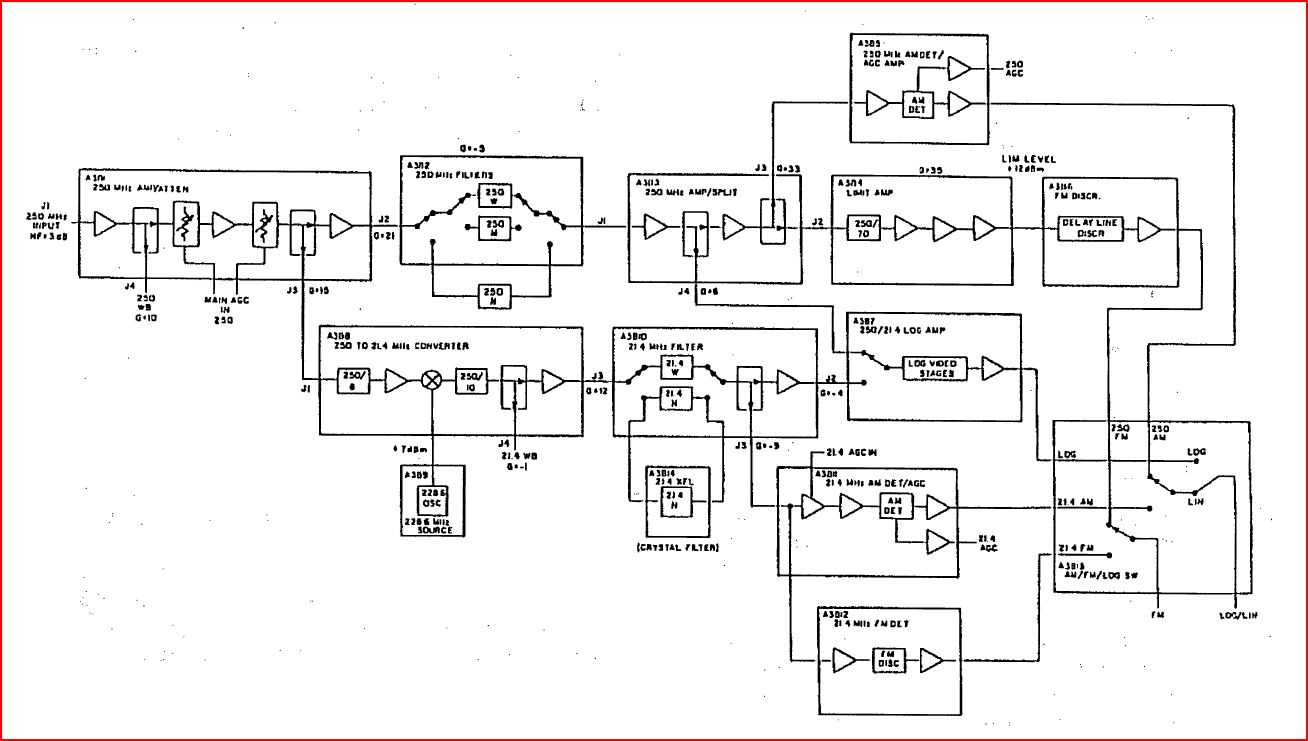
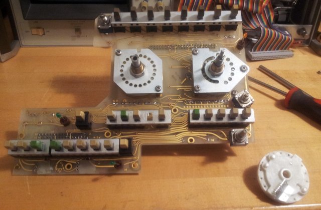
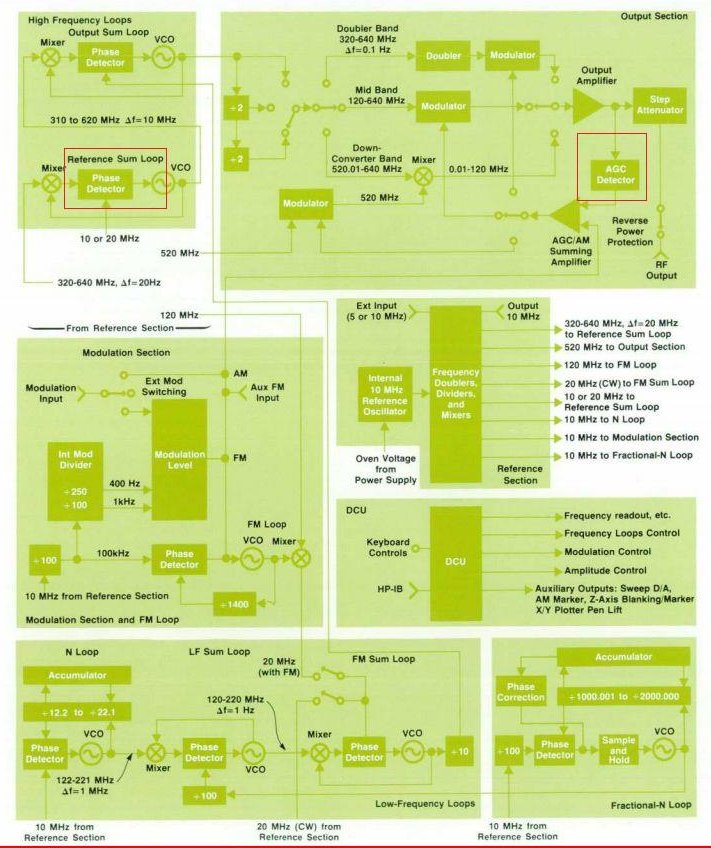
Item (3) – nothing worse that disassembling the IF chain – by all admiration for this unit, the 2nd IF chain is not build for troubleshooting. But, following the instructions, first a check of the control assembly. And, quite to my surprise – a defective transistor switch, using a 2N2905 PNP transistor that provides +15 V power to one of the 24.1 MHz amplifiers – this is switched on and off depending on the BAND setting. The transistor – only had a 2N2904 around, same kind, but a bit lower gain. Well, it works – need to check stock back home in Germany when I get a chance.

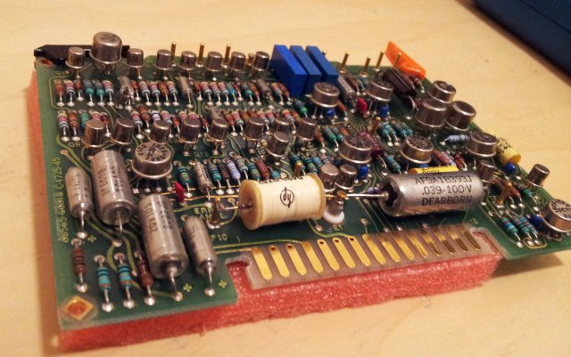
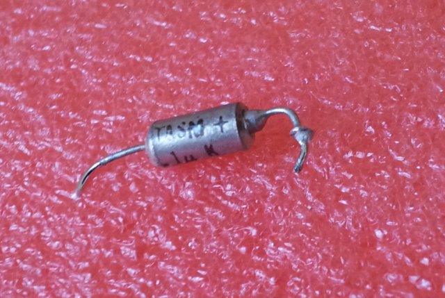
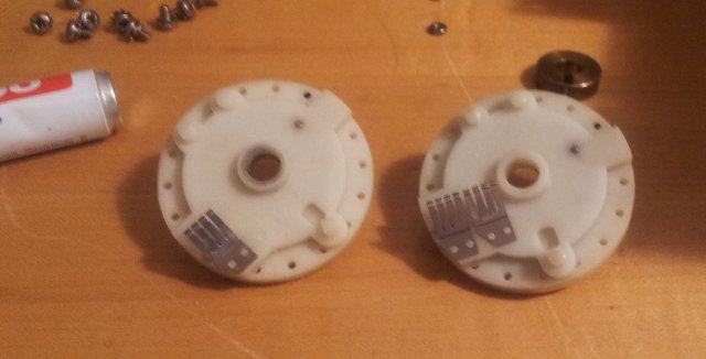
These are the bad guys-
msr-904a more bad guys

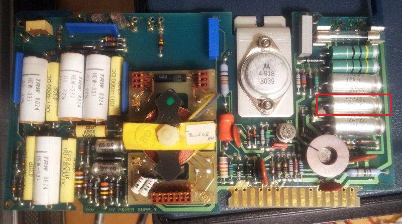
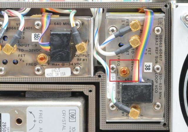
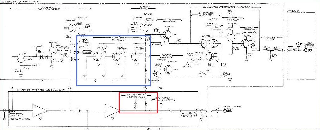
Item (2) – this was “just” a matter of adjustment. Adjustment isn’t all that straightforward – and the manual doesn’t cover everything. Needed to peak the 250 MHz amp/AM detector circuit – there is a tuned amplifier inside, which has and adjustment capacitor not described in the adjustment instructions – fortunately, pretty clear from the schematic.

Item (5) – turned out to be a 1458 opamp not working properly, replaced. Pretty easy – most of the integrated circuits are in sockets. Sorry, no picture of the defective 1458 😉

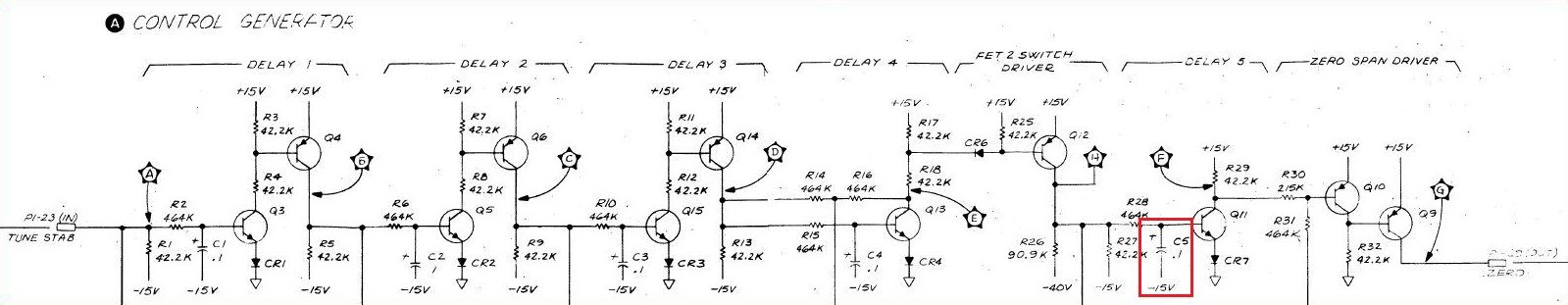
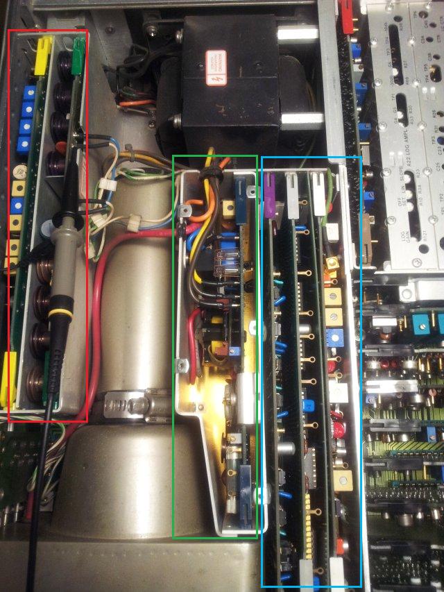
Item (4) – added a good Chinese brand SIP reed relay, PAN CHANG SIP-1A05:
sip-1a05

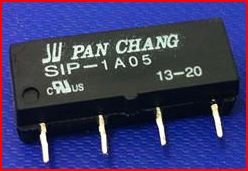
Routed a wire with the EXT signal (low when activated) to the YIG driver board. This is now taking the 100 n cap out of the circuit, unless the EXT mode is active. Added a protection diode, to avoid voltage spikes damaging the TTL circuit driving the reed relay.

msr-904a a7b3 yig driver

msr-904a yig driver bw limit ext mode

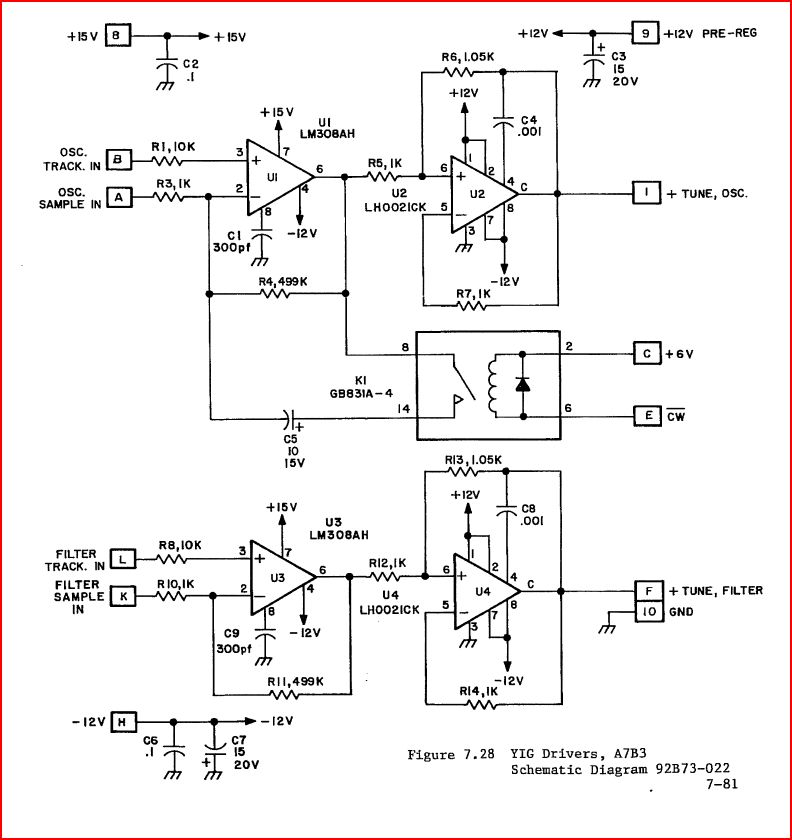
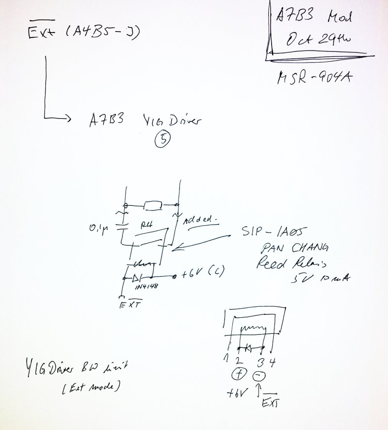
The 100 n cap and reed relay is installed parallel to the R4 resistor – same as for the C5 capacitor, which is activated in CW mode.

Micro-Tel MSR-904A Microwave Receiver: manual found!

I had almost given up. It seemed that a full manual of a MSR-904A would be perfectly unobtainium. Well, most secrets of the MSR-904A were reverse engineered anyway, but there are some subtle details and adjustments – just a bit arbitrary to do without proper documentation and at a least a bit of insight into the thoughts of the designers of this marvelous apparatus.
One reason might be that these units were long banned from export and mostly governmentally owned. Eventually, the units reached the secondary market, but the manuals, they rest in some archives, or have long been disposed off by the agencies.

Now, to my greatest surprise – a copy of the manual has been located – in Germany. The paper copy, it seems to belong (or have belonged) to a certain H. S. in Webenheim, a place, a mere 72 miles form my German home.
Another fellow German must have scanned this, and again, another fellow, send it to me, electronically. Albeit, not for free, but, fair enough.

msr-904a manual

It is complete with all adjustments instructions, explanation of how it works, parts list, and SCHEMATICs.

Here, a block diagram of the IF chain – without the 160 MHz 2nd IF output option (by conversion of the 250 MHz 1st IF using a 410 MHz LO) installed in the unit I have for repair.

msr-904a if chain

Screening through the manual, the complexity of the thing is pretty much amazing. All without any controllers or processors – but there is at least one programmable part, a PROM that has the filter switching matrix. Come on, this could have been done with a diode matrix!

AIOM: updated schematics, differential input bias, high-impedance input protection and amplifier

Some progress, with the universal analog input output module, analog response analyzer, or line tracer, digitizer – however you want to call it. Added a few features – a bias supply for the differential input, and a high impedance amplifier (and a bit of protection circuitry) for the single-ended input.

First the bias supply – to allow a wide range of input voltages, say +-20 V (even below ground and well above the positive rail), we need a resistive divider network, and this needs to convert a differential voltage (with absolute voltages centered around ground), to a differential 0 to 2.5 V input, centered around 2.5 V (the internal bias of the ADC). A little calculator is used to find the right resistors and bias voltage. About 2.65 V will do the trick, for the desired input range, and resistor combination. Bias current is just about 1 mA or so, easily sourced/sinked by a OPA703 opamp.

adc input bias calculator

This input is mainly designed to sense low impedance sources, e.g., current shunts or supply voltages (lead compensation, or similar configurations). So the ~50 k input impedance will be perfectly fine.

aiom schematic 1 of 2

aiom schematic 2 of 2

The general circuit, nothing really exciting about it – the AD7712 has a 8 MHz crystal, will run easily up to 1 kHz conversion rate. But mostly, it will be run at 50 or 60 Hz, to suppress any mains related noise, or even at 10 Hz.

A quick test showed that the USB communication is working (using a JY-MCU ATmega32L minimum board) – just waiting for some long waiting times and train travels to write a simple user interface, to control the outputs and the data acquisition by Windows GUI. For plotting and data analysis, I will resort to gnuplot and/or R, not re-inventing the wheel here. Maybe a simple preview screen.

HPAK 8569A Microwave Spectrum Analyzer: some adjustments, an ultrastable 10 Volt reference, GPIB test- repair completed!

The manual for the 8569A describes a series of performance tests – not all of them were completed, but most. Fortunately, the IF chain doesn’t need adjustment. Still, it took nearly three hours to get the YTF tracking, the A/D converter/digital display section and other display related circuits adjusted. The log amplifier was carefully tested as well, all perfectly in tune.

The most amazing find – the internal 10.0 V reference was found at 10.00004 V. That’s +4 ppm – most likely, better than the voltmeter I am using to measure this.

The reference circuit, according to the datasheet, is uses a regular HP/RCA low noise opamp of the late 1970s (selected 741), and a +-10 ppm/K 1N827 temperature compensated zener. As it turns out – the actual part used is a 1826-1058, an OP-02 equivalent (0.65 µVpp noise, 8 µV/K drift), much better.
Resistors in blue frame are +-10 ppm/K tempco. Others are regular, +-100 ppm/K resistors.
The circuit layout – very much refined, a marvel of analog engineering – guard traces all around!

8569a 10 v reference circuit

It is run at exactly 7.44 mA, using the 10 V reference to set the diode current – to minimize the temperature coefficient. See this diagram from the 1N827 datasheet:
1n827 tempco vs zener current
Seems that after 34 years of aging, it is perfectly stable now.

Back-up of the internal EPROMs (4x 4 kbyte!) stored – just in case they fade out over time.

Last step – test of the GPIB functions – and, no issues at all.

Writing to the machine:

8569a hello world

And receiving plot data back (two signals, close to 100 MHz, -10 dB):
8569a plot

At its final place, for now, on top of a 3585A – total of almost 200 pounds of test equipment. Hope the bench won’t cave in.
8569a working

HPAK 8569A Microwave Spectrum Analyzer: tuning stabilizer/tickler repair

After fixing the display and front panel related issues (attenuator, “0 dB” indicator), the only major defect remaining so far is the tuning stabilizer circuit. Once the span is set to below 100 kHz, it is activated – and sets the unit to zero span, rather than the span selected, permanently. Only when the stabilizer is disabled (there is a button on the front panel), the span is back to normal.

The source of this issue – most likely, the A14 tuning stabilizer assembly. Switched the board (part number 08565-60018) with the identical board of a 8565A – and, as expected, the zero span issue is gone!!

Now, we just need to fix the board.

The description in the service manual is actually pretty clear – the circuit uses a 1 MHz harmonic sampler, to keep the frequency of the LO stable. The initial lock is achieved by setting the analyzer to zero span, finding a frequency close to 1 MHz that represents a lock point. This frequency is controlled by a voltage, and a very long lasting sample-and-hold is used, than employs a special construction of a HP reed relay, and a PE/PTFE(?) lowest leakage capacitor – the white coil in the front, left, and the the capacitor, front, right – in the middle, a PTFE isolated post, going to a FET gate.

8569a a14 assy 08565-60018

Certainly, a very special capacitor. Once this is achieved, error voltage of the sampler is used to steer the LO, and the analyzer is returned from zero to normal span mode.

The sequence of all these steps – controlled by a very interesting chain of transistors, resistors, and capacitors – nowadays, just a few lines of program code… but, nothing better than a handful of discrete high quality components.

The “control generator”, see schematic below – it is not controlling the sequence properly – and, again, a defective cap. 0.1 µF (!), tantalum – red frame; a few 100 Ohms – near short. No way that this can get charged, and let the sequence proceed.
08565-60018 control generator schematic

Replaced it, with a regular 0.1 µF cap (why did they use a tantalum??), and: A14 assy working again. 20 kHz span, 10 kHz resolution bandwidth. Working just fine – at all frequencies up to 20 GHz, the highest I can check here.

8569a working stabilizer 20 khz span 10 khz res bw

The black sheep (date code: 1980, week 7):

8565a a14 culprit

We can’t argue that they didn’t skim on parts – at the time, certainly, one of the best 0.1 µF tantalums available.
Parts list specifies 150D series, MIL–PRF–39003 mil-spec qualified high reliability hermetically sealed cap:

150d tantalum

HPAK 8569A Microwave Spectrum Analyzer: front panel repair/re-build

The easy of use by the three-knob operation mentioned before – it has a downside: a very complex front plate assembly. And this might be the reason why more modern units almost exclusively use single-axis rotary encoders, often only one single encoder to operate all functions, per unit. The multi-turn-coupled-limited-synchronized-geared movements, just too complex and too expensive, too heavy, too laborious to maintain.

The front panel controls – as delivered.
8569a front panel rhs as delivered

The 8569A, 8569B and 8565A all use very similar front assemblies – only seem to differ in the print and in the exact shade of the label colors. And these assemblies use plastic parts – knobs, wheels, and so on. After 30+ years, no wonder, aging has visible effect, and parts become brittle. Common defects are broken-off sliding contacts. Not a big thing, can be fixed (re-attach the contact with M1.2 screws).

The attenuator and “0 dB” warning indicator – these are located on the same rotary cam, same contact pair. And, you bet, the corresponding wiper contact – broken off-missing.

Well, having rebuild some of these assemblies for other repair jobs before – the only way to fix this will be to take the assembly apart, almost fully. Actually, if all screws are kept well-sorted, not really such a big effort as is sounds. Some hours, but then it will be working again.

8569a rebuilding the from assembly

In addition to just the repair, all contacts and surfaces were thoroughly cleaned, by various means: DeOxit D5, a good eraser, isopropyl alcohol. For the painted surfaces and parts, use 40-50% isopropyl alcohol only, and a rather soft or medium-hard brush, to avoid damage to the paintwork.

The replacement cam (on the right) has two wiper contacts, the defective part, only one – the plastic fingers holding it down became brittle, and it eventually broke off.

8569a attenuator selector cam

Here, the result: the rebuild assembly. From earlier repairs, the remaining contacts should last – somehow, no all are susceptible to breaking-off; or it is just the amount of use they get – at least, I have some units fixed with small screws holding down the contacts, and there have since been working better than before. Therefore, I am not too worried about more contacts failing in the near future.

8569a rebuild front panel assy

Note: as it turned out, also the 12 dB vernier attenuator encoder had a partially broken off contact – can be fixed with some epoxy glue, but I rather replaced the encoder, with a spare from the parts unit.

HPAK 8569A Microwave Spectrum Analyzer: display fix, A6 assembly

No display – this can be bad news, because spare CRTs are hard to come by. Let’s see what we can do here.

Overview of the assembly – red: XYZ driver boards; green: high voltage (and other supplies) for CRT; blue: digital circuits-video signal generator.
8569a display unit

The digital part and XYZ driver – seem to be fine, can get a nice video signal when probing around.

Well, the HV power supply – no signs of life. You can easy check, just switch off the unit – there are two neon bulbs that discharge the CRT – but in the current case, all remains dark.

Removed the HV power supply assembly (A6) – fuse is blown! A quick look at the schematic:

8569a partial schematic a6 assy

Only three options, either the 26 V filter, the transformer, or the Q1 driver transistor. Driver transistors are a common fault – high voltage transients can damage them. But, Q1 is testing fine.

The transformer, looking good.

The filter – well, there we go, a classic fault, a defective cap.

8569a hv power supply

This is a 50 µF, 50 V, Sprague (now: Vishay), 30D series. Date code: 1980, 26th week! “Made in USA”

8565 30d cap

This exact series – still available today, after nearly 35 years! These don’t fail so easily, but the A6 assembly, there will be some stress on these parts. The failed part is capacitor C2 – the part that is doing most of the filtering. Maybe it would be a good idea to put a 1 µF foil capacitor in parallel with the electrolytic caps, to absorb the spikes…

For the time being, just replaced the defective cap, and ordered some 105°C rated long-life caps. 30D series caps aren’t cheap. So I settled for a Kemet brand type. Will be good enough.

After some soldering, powered the thing on:
8569a working display

We have a working display!! And, it is actually a very good CRT – no signs of wear! Most likely, sitting in some lab at Iowa State University, as one of the labels on the case suggests, and then, stored away in a nasty shed or garage for years.

Now, repair can move forward – without a display, at would be only half as useful.

The culprit, and the dead fuse:
8569a hv pwr supply culprits

HPAK (HP Agilent Keysight) 8569A Microwave Spectrum Analyzer: a great find, 10 MHz to 22 GHz, and some spare parts at hand

Two weeks ago I spotted something on xbay, a 8569A spectrum analyzer, for parts or repair (“powers up, no display”), at a very reasonable price – just a bit above USD 300. This is not much more than the parts value of the 70 dB attenuator of this unit, so, a great deal in any case. The pictures shows a really beaten-up unit, black dirt all over it (mould?), and corrosion. At least the connectors seemed to have caps on them, fair enough. And it has option 1, a 100 MHz comb generator, good out to 20 GHz.

Unit as offered… doesn’t look very appealing.
8569a offer

Good news: I have a severely damaged 8565A here (broken frame, but still full of good parts), as a donor unit – looks like it is a unit that had been buried under tons of heavy stuff, or had a truck driving over it, a heavy truck. And, it doesn’t have a CRT.

8565a donor unit

The 8565A, 8569A and 8569B analyzers – these have a really easy to use design, three-knob operation, and are the best analyzers, from my point of view, for any general service and adjustment work, at any frequency above a few MHz. With resolution bandwidth down to 100 Hz, also up for some more special tasks. Sure, there are the 8568 and 8566 units (I also own a 8568B), but these are bulky, and you always need to push buttons AND turn knobs – more like for a cal lab or really high precision characterization work.

Plenty more modern analyzers exist, with LCD display, and all kinds of software features. They come at a price, and once you have experienced the responsiveness and easy of operation of the 8569 series, fancy LCD screens and color buttons can’t really be the reason to consider anything else. Good units, fully functional-refurbished, go for about USD 2-3k.
For general-purpose, low budget work – if you are looking for a 20+ GHz analyzer, there isn’t much that goes for less than 10k used, or 30-50k new. Some of the later, semi-portable 856x series might be an alternative. However, these have a rather small screen, just about 3.8″ diagonal, for the spectrum display, while the 8569B has 5.5″, and an electrostatic CRT, of excellent brilliance.
Also, keep in mind that the down-converted output can be easily converted to digital data by SDR, to recover even the most complex modulation schemes. No need to pay extra dollars to get custom plugins for modern analyzers. Such things pay off for the big corporations, but if you are up for special tasks, there is no way around dealing with some software, anyway.

Currently, I use a 8569B in the workshop back in Germany, and here, in the US, I rely on a 8565A – which is essentially the same RF hardware, but has an analog storage display (variable persistence), rather than a digital display, like the 8659B. Also, the 8565A doesn’t have GPIB or other means of data bus, all computer-controlled measurments require the use of a A/D D/A converter unit.
So, it would be good to get the 8569A working, and eventually, sell-off the 8565A.

Historically, it seems the 8565A first appeared in about 1978. Looking up in some old HP catalogs – the 8569A appeared first in the 1982 edition (marked as “new”); quite surprising, because the unit I have here has a much earlier serial (1980) – and also the parts data back to end of 1980.

8569a serial
No doubt, seems to be a rather early unit (take the first two digits of the serial, and add 1960 = year of manufacture).

HP-Cat-1982-8569a

HP-Cat-1983-8569b

In the 1983 edition, HP already has the 8569B, with virtually identical specs. Quite interestingly, the 8565A (with the analog storage display!) remained available, in parallel with the digital-display 8569B, for many years – up until 1988 (at USD 34k, including option 1). The price difference was rather small, just about 10% (about USD 3k) more for the 8569B, with the much better display, and digital/automated control capabilities.

If you study the inner workings of the 856x in detail, it is also evident that a good part of the circuits were taken from 8555A analyzer, introduced in about 1970….

After all this, the analyzer arrived – well packaged. And first downside of it, it is 30 kg, 65 pounds, plus packaging. But hey, who needs to carry spectrum analyzers of this kind around – it will rest on the microwave test bench, along with generators, counters and so on, some 100s of pounds anyway.

Well, plugged it in – the display is really dead, but the frequency display is on. Powder supply is good. And, the X-Y output – when connected to a scope – you can actually get some signals, and it is sweeping. There is hope.

After some probing and basic tests, these are the items found so far:

(1) No display. However, there is a display signal on the deflection plates, and it is looking sound, so the digital display generator seems to work just fine. Just the CRT isn’t. Might be hard to fix, if the CRT is at fault – I can’t see the cathode glowing….

(2) The attenuator at 60-70 dB, and “0 dB” attenuator light at the front panel – not working (missing 20 dB attenuation; light off even when attenuation is set to 0 dB.

(3) Mechanical defect of the span knob – general mechanical soundness of the front panel. Will need very through cleaning, aligment, etc.

(4) Something is wrong with the tuning stabilizer, engaged at below 100 kHz span – when it is activated, it sets the span to zero, and never comes back, unless the stabilizer is de-activated.

HPAK (HP Agilent Keysight) 8662A Synthesized Signal Generator: ref sum loop adjustment, output amp/peak detector repair

Introduced in about 1980, the 8662A is a marvelous machine, it is an ultra-clean signal source, with very low close-in noise. This is the kind of oscillator used as a reference for phase noise tests, narrow channel receiver testing, and so on. Just a quick glance at it inner working, and it is clear that only the most brilliant engineers must have been working on this apparatus in those days. Sure enough, this did not come cheap, about 30 k$ in 1981, something like 75+ k$ nowadays…

Even more interesting, these machines are still in use today, and are still valued for the same reason – hardly any synthesized generator exists that has similar close-in noise.

The block diagram – essentially, there are two ultra low noise switched inductor osciallators that form the reference and output sum loops, together with with some fractional and n divider circuitry, to allow for the fine resolution. The output sections has a heterodyne band, and other bands derived by doubling or dividing the 320-640 MHz fundamental output of the output sum loop oscillator.
8662a block diagram

As with all wonders and complex machine, they sometimes stop working. This one had two issues reported, inaccurate output power (and error #10B – ALC error for some frequencies/settings), and a ref sum loop unlock condition at certain frequencies. The latter issue had been persisting for some time, but the ownder didn’t use it at the critical frequencies, the ALC loop error just recently seems to have come up, for now external reasons, apparently, during a measurement.

(1) The output sum loop A6A5, error #06. This turned out to be a drift issue, of the low noise REF oscillator. This had drifted out of pretune span, and needed just very slight adjustment of the tuning screw (under a heavy metal cover, rear panel of the instrument). Such adjustment is not mentioned in the manual, but easy enough, set the generator to 640 MHz, check that the pretune is properly adjusted (adjustment is done for -3.75 V at 320 MHz), introduce a -34 V tuning voltage signal, and adjust for a frequency a bit above 640 MHz, say, 642.5 MHz, to give the phase loop a bit of room to operate.

08662-60417 oscillator

Great care must be exercised, because the adjustment uses a copper (!) screw – red frame in the above picture, most likely, acting as a capacitor vs. a metal surface inside of the unit (don’t open up these oscillators – they are wraped in Mu metal or similar exotic material). Don’t overtighten the retaining nut, copper is pretty soft.

After that, the ref loop is stable again, even when sweeping through the full band, for some hours.

(2) The more tricky part, as it turns out, the ALC loop. This is implemented on assemblies A4A1 (which has the peak detector), and A4A7, the ALC control, this has a DAC, to set the target voltage, and a regulator, to keep the output signal at the level set by the DAC output.
8662a a4a7 probing
After some time of probing around, and substituting the input of the A4A1 assembly by a calibrated 100 MHz signal, it is clear that the A4A1 peak detector delivers insufficient voltage, and that the voltage is frequency dependent.

A quick glance at the schematic:

8662a output amp

Blue frame – the bandwidth limiting circuit, enganged at below 10 MHz – first guess: something is at fault, in this circuit. Well, unfortunately,after even more probing, and even swapping some transistor (they tested good but you never know) – the focus shifted to the part in the red box. The peak detector diode! This is really bad news, because it is part of the output amp microcircuit, part number 08662-67008. Carefully desoldered, and checked – the detector diode has 0.3 V forward, which is fine, and 0.7 V backwards – this is a far too low reverse breakdown voltage. Something must have happened with this diode, maybe, it is just age. So, I openend up the circuit (the lid can be lifted off with a knife, glued on with silver epoxy), and inspected with a microscope – no obvious defect, all kind of nicely wire-bonded parts on sapphire(?) substrate – nothing I can fix with the tools at hand.

08662-67008

But, as luck comes along, found two of these circuits on ebay. Very mysterious. They look like old and used and ripped out of the boards (with a screwdriver, not by desoldering), and I suspected that the two might just be damaged parts – but 14 days right of return were offered, so not an issue. Even then, it doesn’t really make sense to rip the out of the board, every reasonably skilled and knowledgeable person would rather desolder them carefully, and fit a spare. However, these spare still had the through hold plated vias on the connectors, from the board. Glad the feed-throughs at the bottom of these microcircuits are so sturdy! Well, the only explanation I have – someone saw the golden parts, on some odd circuit boards, and only wanted to keep the gold, but not the boards. Fair enough.

And, this is almost the end of the story, the spares arrived within a few days, and I cleaned them up, and fitted the most “used” looking 08662-67008, and, quite to my surprise – working just fine.

The only thing that remained was the amp bias adjustment, the offset adjustement (both on A4A1) and the CW power adjustment (A4A7) – also checked the other alignments of A4A7, but they were all still fine.

In the end, still one output amp in the box, for the next 8662A, and the current one, back alive.

AIOM – Analog Input Output Module: the low-voltage low-current SMU

Quite frequently, I encounter rather large stacks of system power supplies and multimeters to test various types of equipment or circuit prototypes. Often, voltages are just in the 0..10 V range, sometimes, up to 40 V, at small currents. The response of the ciruit is then measured, often, after conversion to a voltage, or as a frequency, etc, with a counter.
This all works, but consumes space, a lot of power, heavy lifting, etc.

Therefore, what is needed, is a kind of Swiss Army Knife, a ADC-DAC unit, with some capable software, a small box that replaces at least two power supplies, and two voltmeters. Preliminary name: AIOM

Essentially, a small brother of the now very common source measure units, aka, “SMU”s.

Possible uses include:

(1) Test of diodes etc – trace recorder.

(2) Control of sweep generators, synthesizers, analog spectrum analyzers (most of these devices have a 0..10 V tuning-frequency control input, and often, a chart recorder-analog output, +-5 V, +-10 V, +-1 V, or similar).

(3) Test of VCO tuning curves, YIG current drivers, YTF circuits. Special VCO analyzers exist, but no need to block a whole lot of space just for some tuning test, and are too expensive to have multiple units at hand all the time. Often VCO tests need to be done at various temperatures, and over considerable time, to ensure performance of a circuit – multiple small test units will allow parallel testing, at very resonable cost.

aiom scheme draft

Features:

(1) Two 0..10 V outputs, 16 bit resolution, low drift, better than 0.05%; source and sink. Needs to have reasonable low noise.

(1b) Optional, to be added, voltage to current converter (to control current, rather than voltage, 0..10 mA, source and sink).

(2) Two inputs, one referenced to ground, one fully differential +-10 V.

(3) Ramp generator and similar features (rough sine, triangle, square/PWM), in hardware, to allow fast sweeps or steps or PWM-related tests (something like a simple arbitrary function gen).

(4) While the basic design will be kept strictly unipolar, there will be a simple switching matrix, to allow polarity reversal. This will also ensure fully symmetrical tests, e.g., for charge counting-battery test, charge-discharge efficiency tests.

The whole little thing has two parts: the AD/DA converter board (prototype build), and a switching materix (still waiting for some parts).

aiom board

First tests successful, stay posted!

aiom test setup