Si5351A + u-blox M7: Clock generator tests

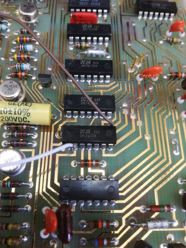
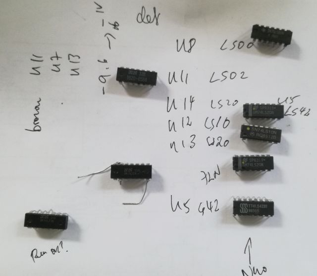
With the Si5351A mastered, time for some tests with the actual application, the GPS receiver (and later GPSDO system).

Two tests were performed:

(1) Using the Si5351A clock generator with a standard, not specifically selected or particularly stable crystal. Presumably, an AT cut crystal, running at 25 MHz.

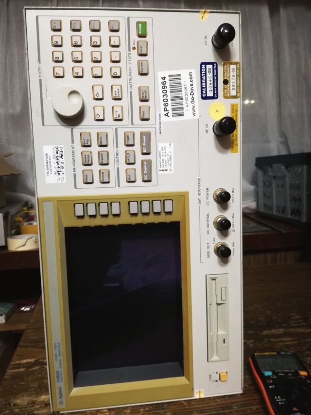
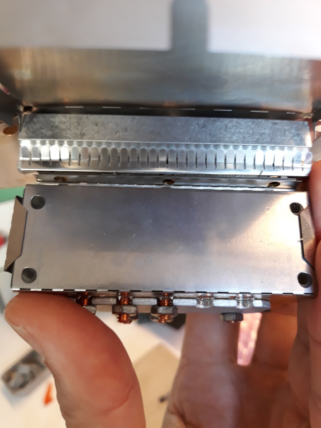
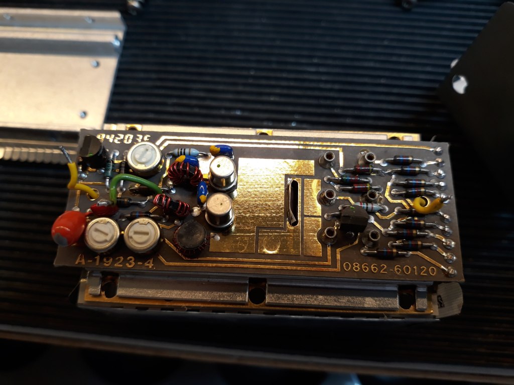
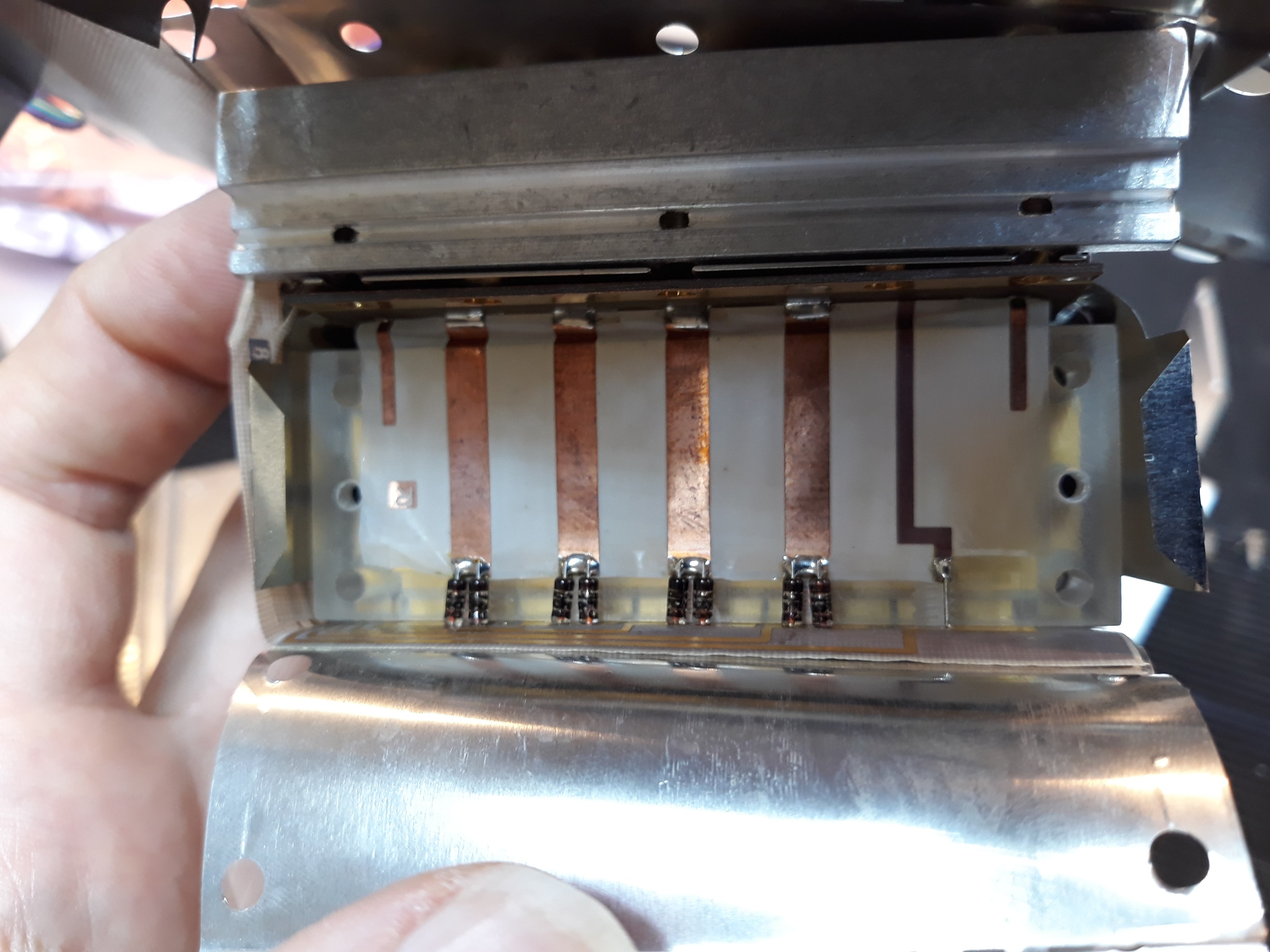
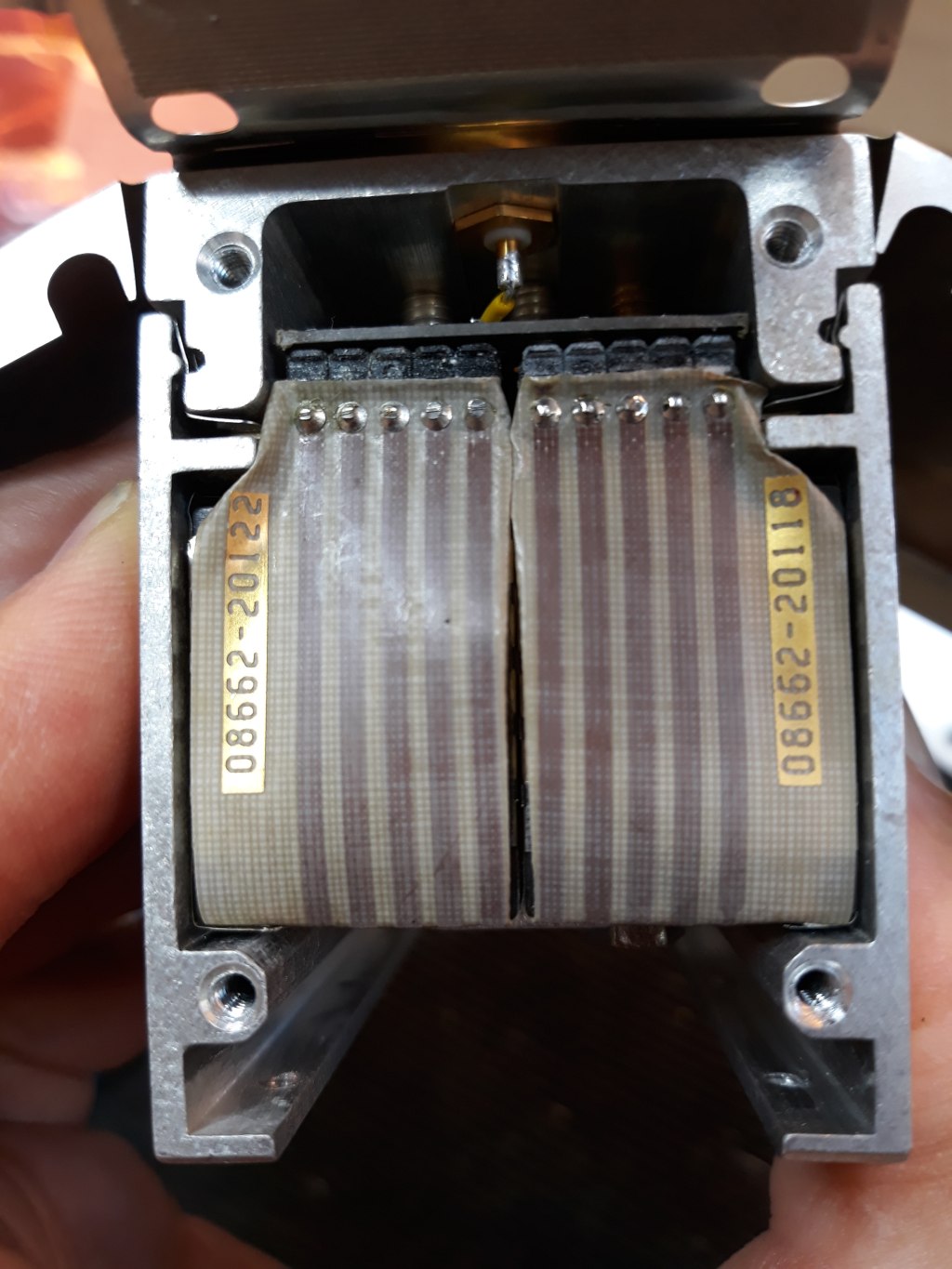
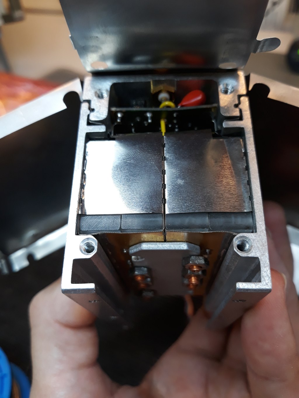
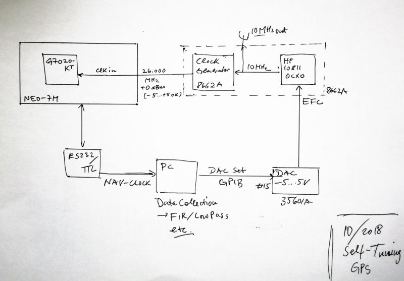
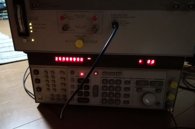
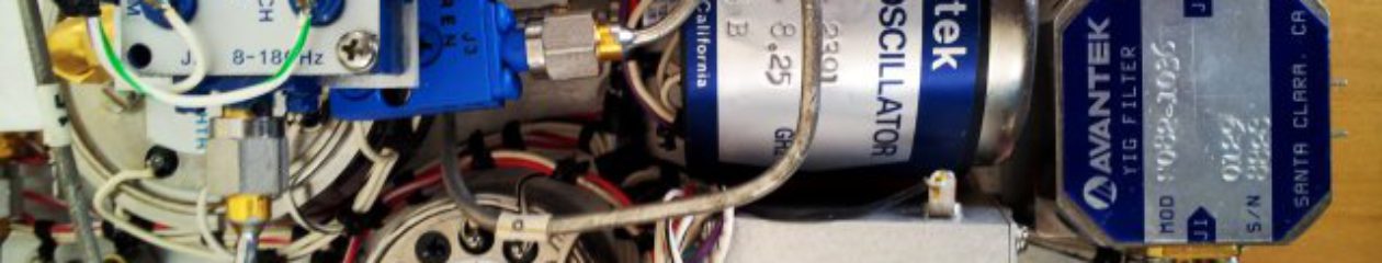
(2) With the Si5351A driven by a OCXO (HP 10811A, part of a 8662A unit – will be later replaced by a stand-alone unit using a HP 10811A with power supply and distribution amplifier, but essentially, to the same effect).

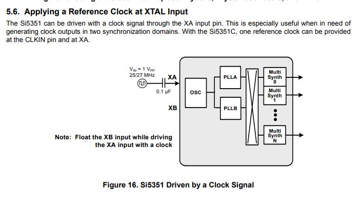
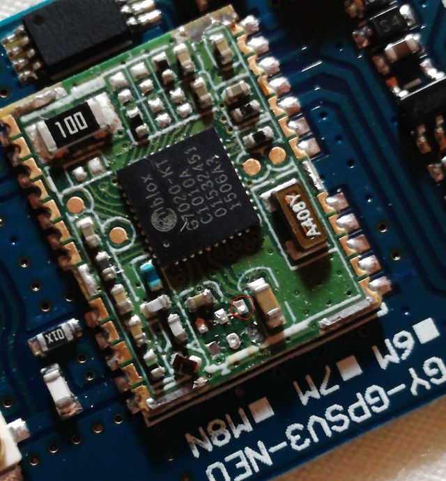
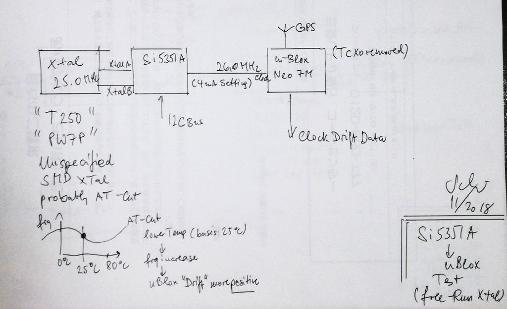
The first test, we need to set the registers of the Si5351A (check the Silicon Labs AN 618 Application Note – check it in a quiet hour, because it has a lot of heavy content…). 25 MHz clock input, 26 MHz OSC0 output – can be achieved by running the VCO at 650 MHz, and integer-only dividers.

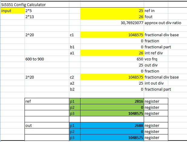
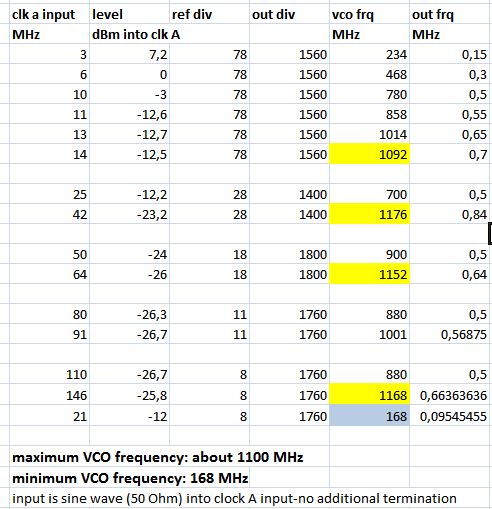
For the calculation, I use a self-made Excel sheet, which allows me to play around with the numbers to figure out the best combination of dividers and VCO frequency.

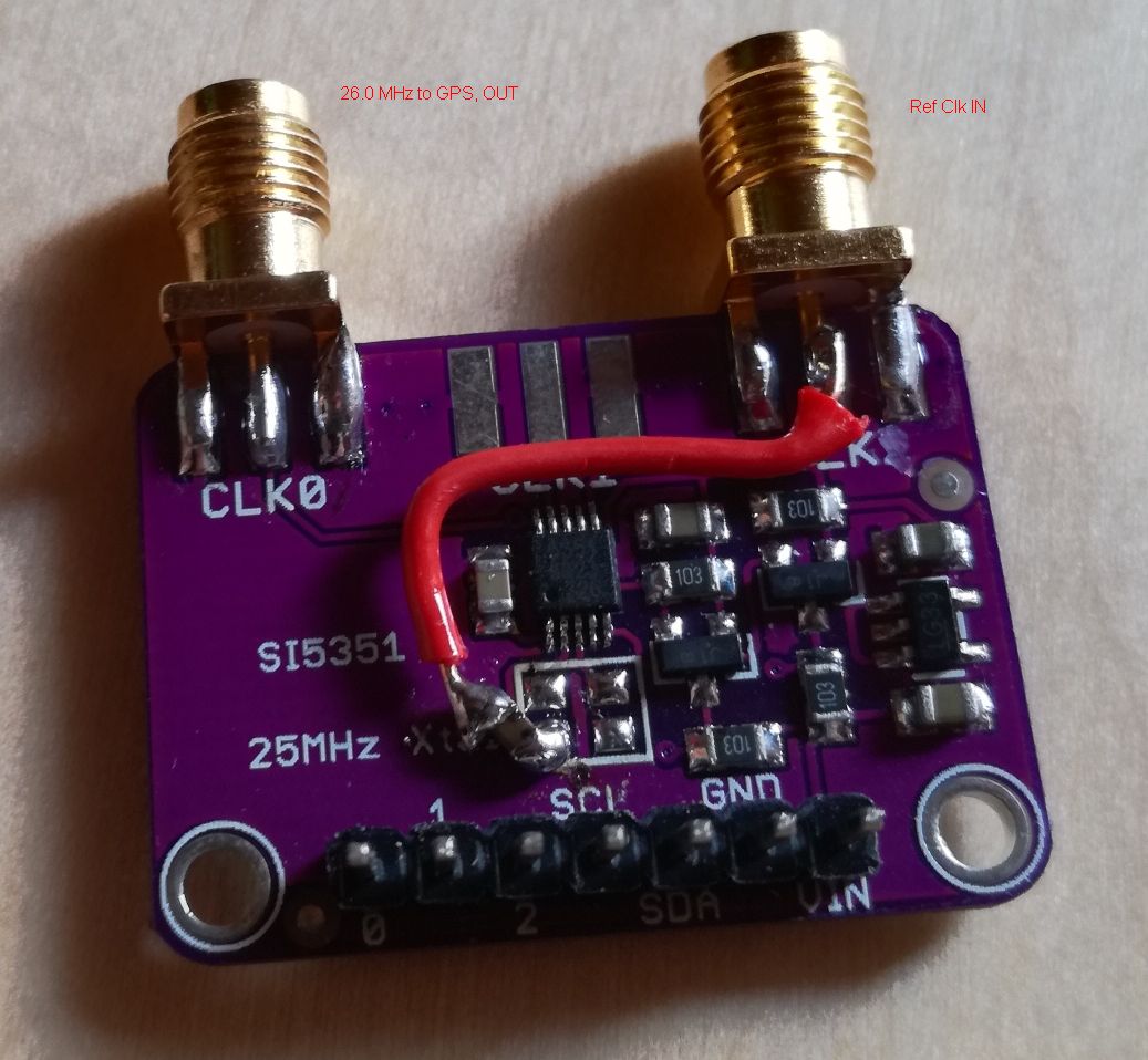
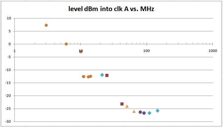
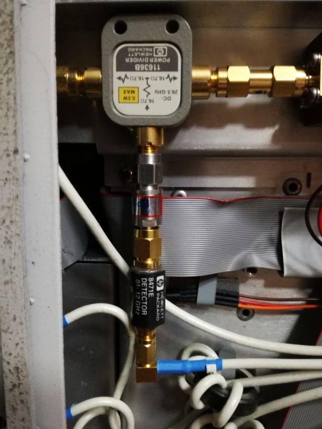
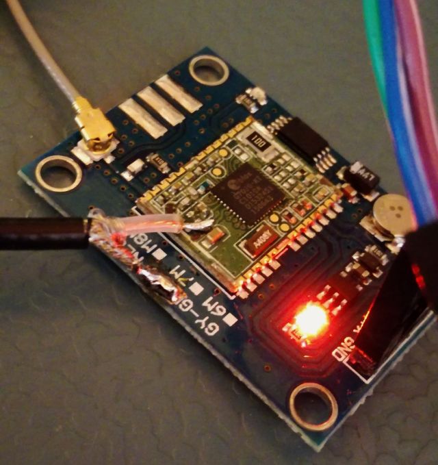
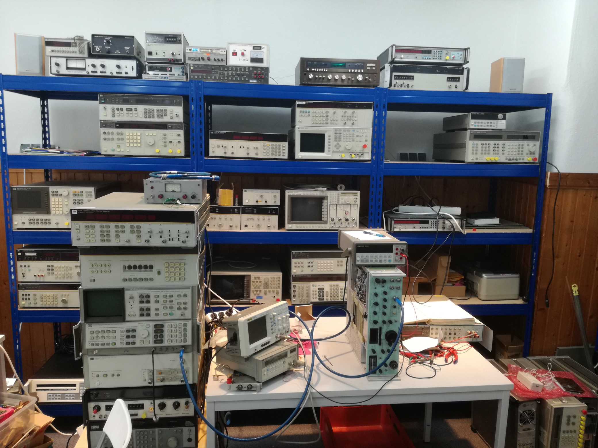
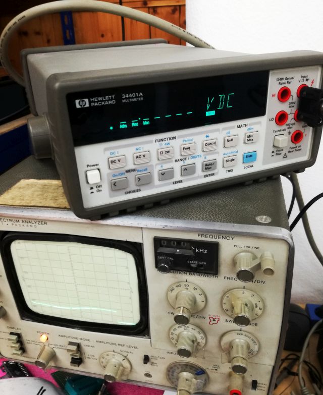
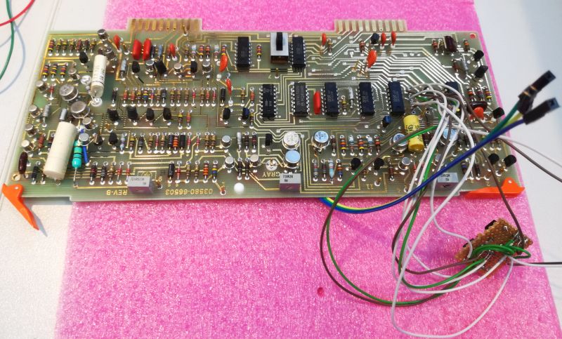
Here, the over test setup:

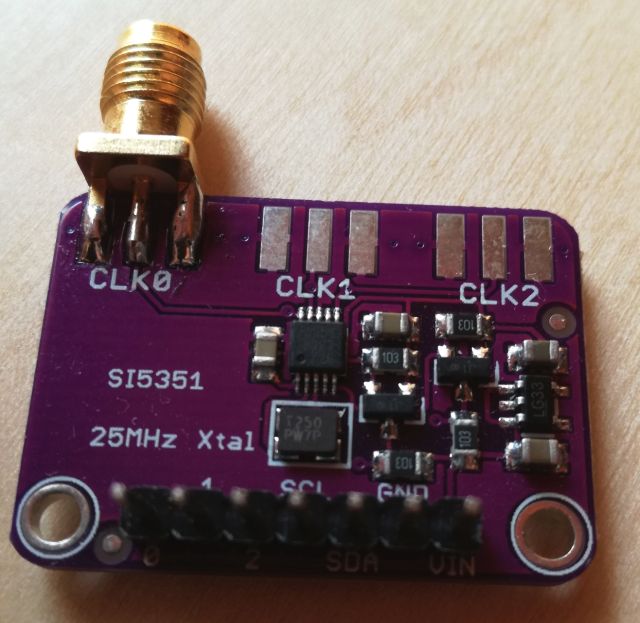
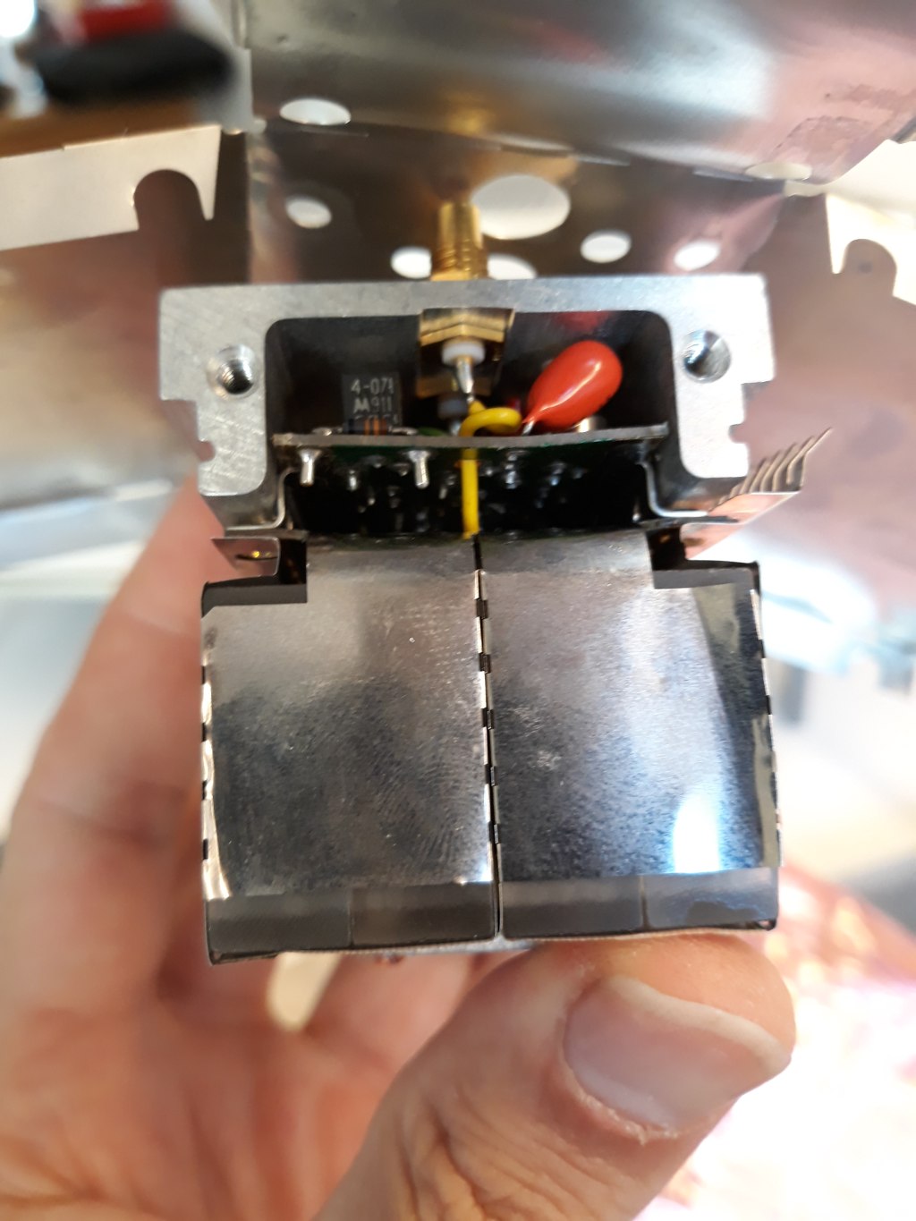
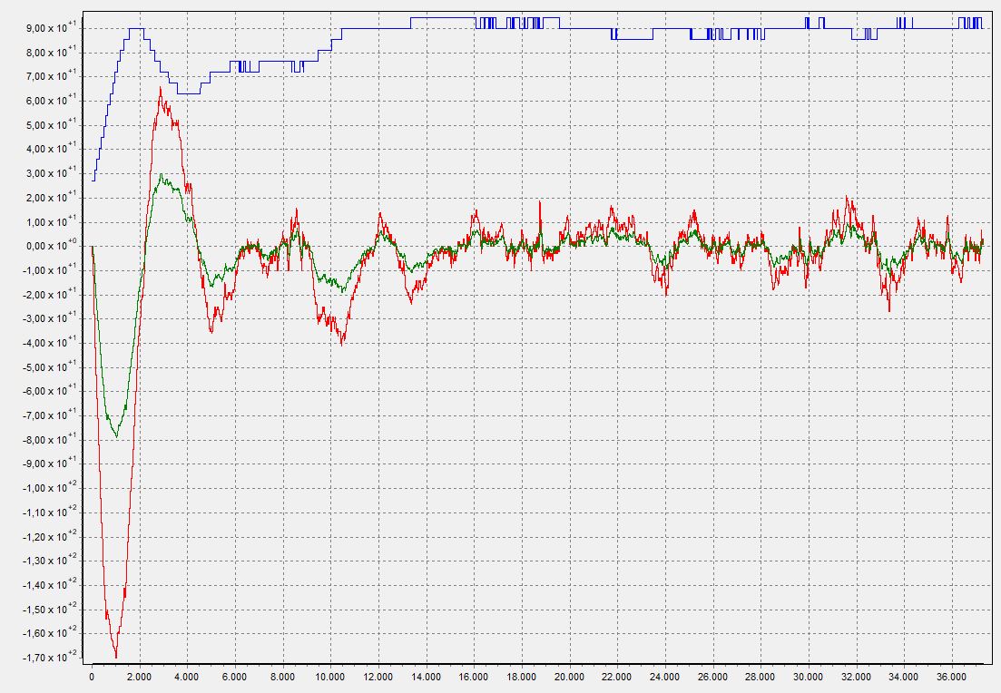
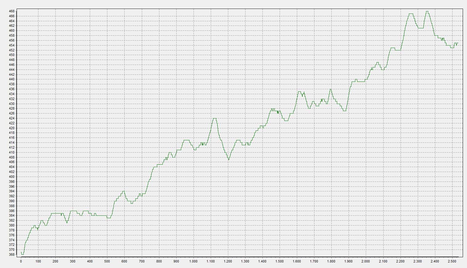
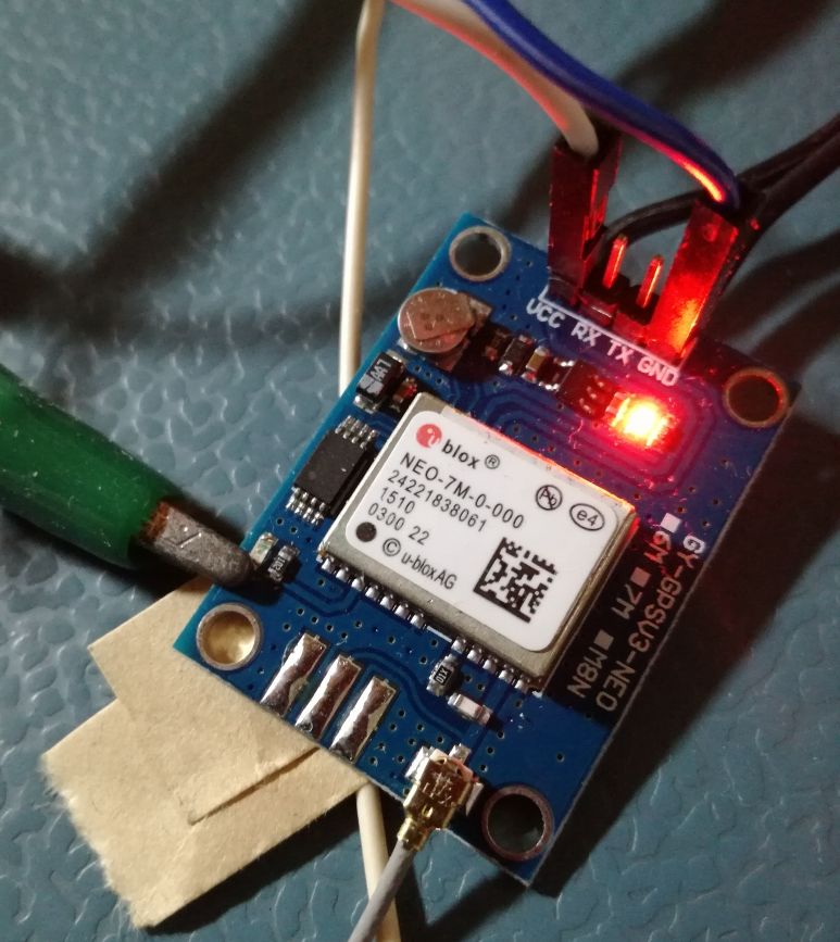
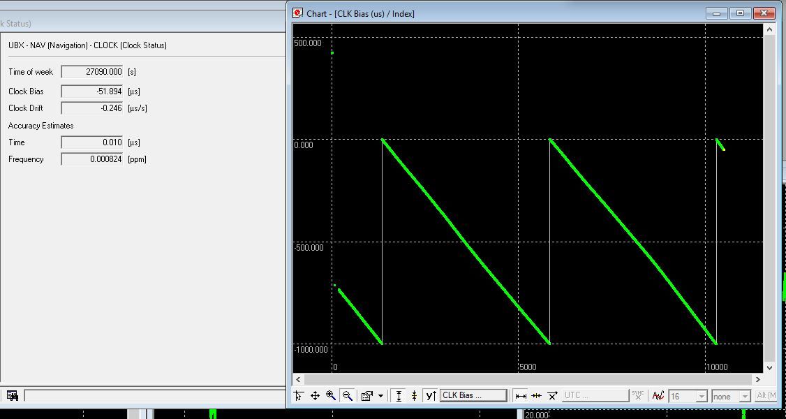
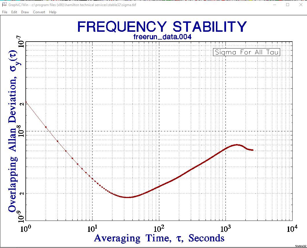
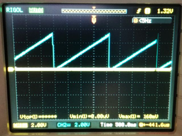
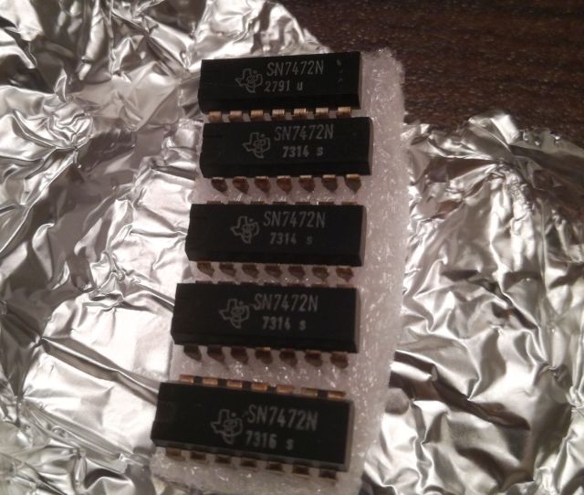
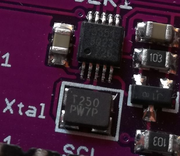
That’s the Xtal used – it came with the board, and I couldn’t find any data on it. Appears to be an AT cut crystal. Starting from room temperature, frequency, will go down with increasing temperature, and up with colder temperatures.

Such temperature variation is easily introduced here in Japan. First, keeping the room at 22 degC by the aircon (A/C) unit, then switching it off overnight (cooling the room by a few degrees, maybe down to 17 degC), then, next morning, heating up again to 22 degC (and a bit more as we had a sunny day).

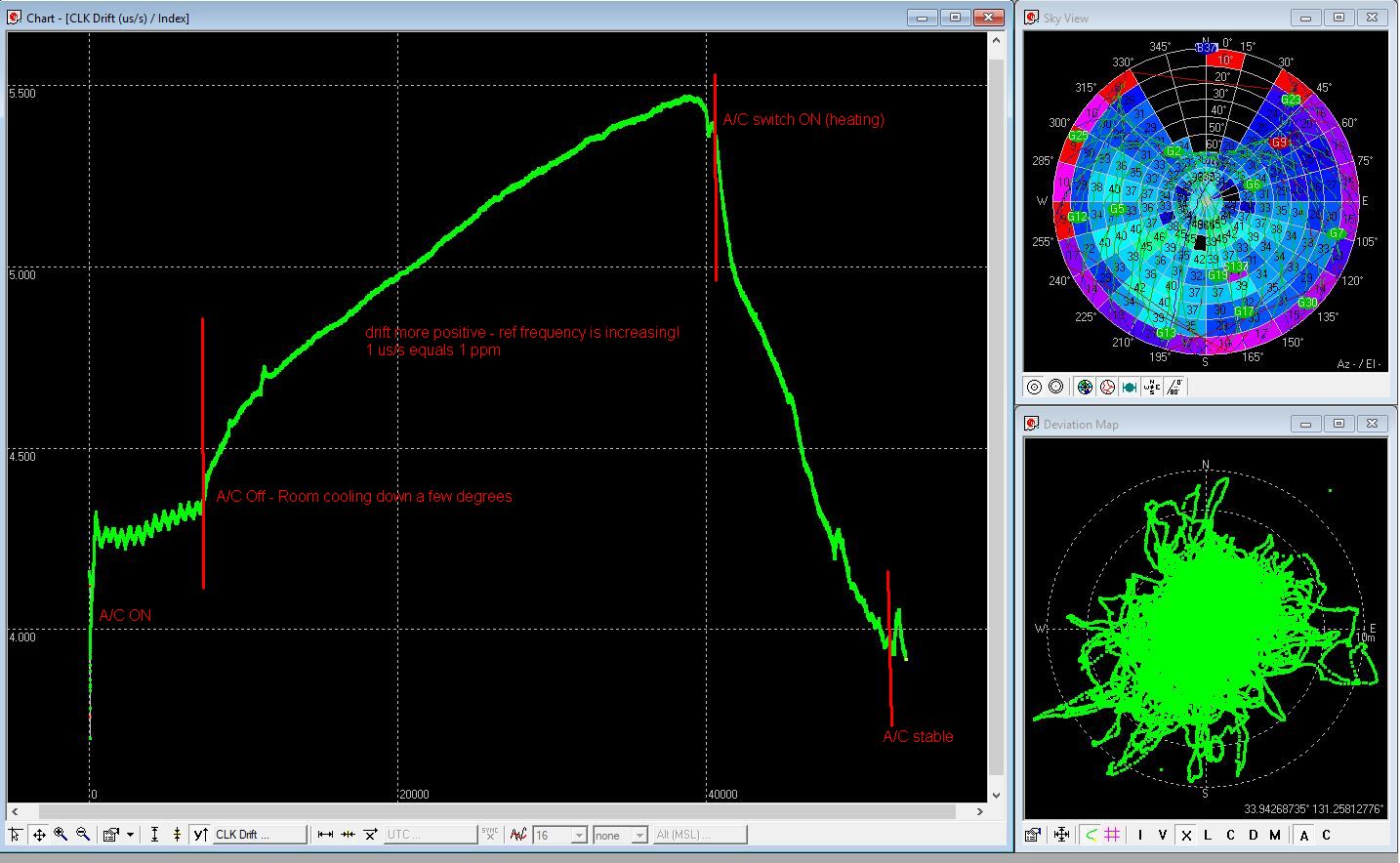
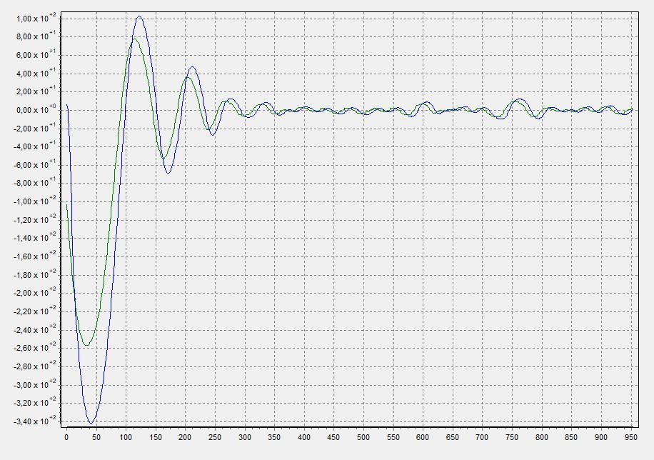
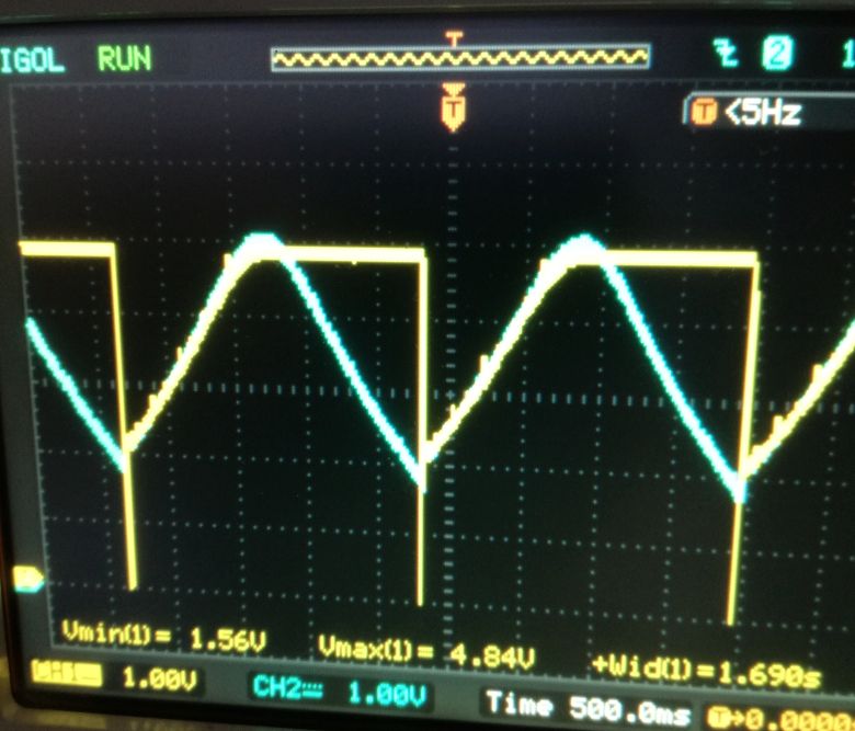
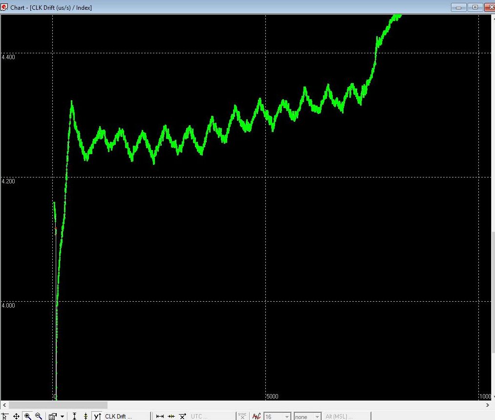
The detail below also shows the small thermal mass of the Si5351A, free-hanging in air. Better to enclose it or to add some thermal mass later, to avoid thermal-gradient introduced noise or instability. You can clearly see the on-off cycles of the A/C unit regulating the room temperature.

After all this study, we find out that we can use the GPS and Xtal as a quarz thermometer (such thermometers really exist!)!

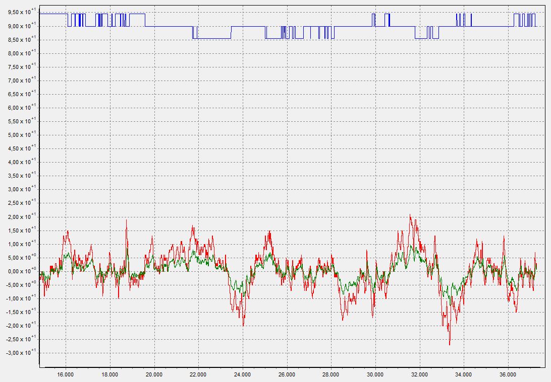
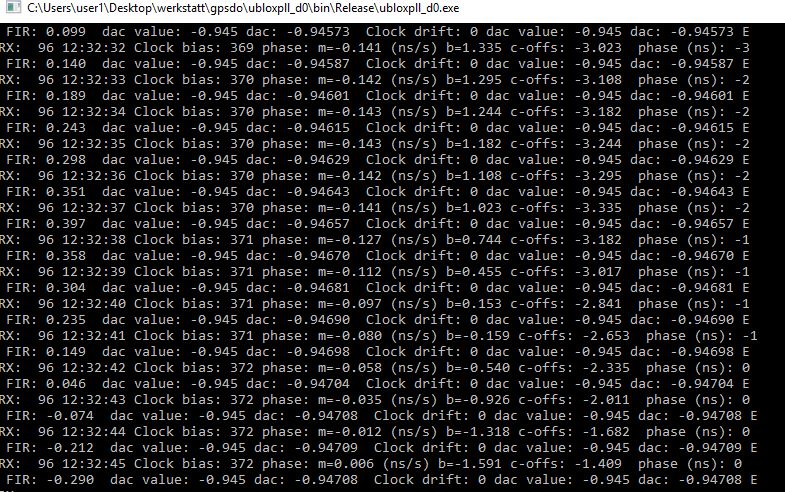
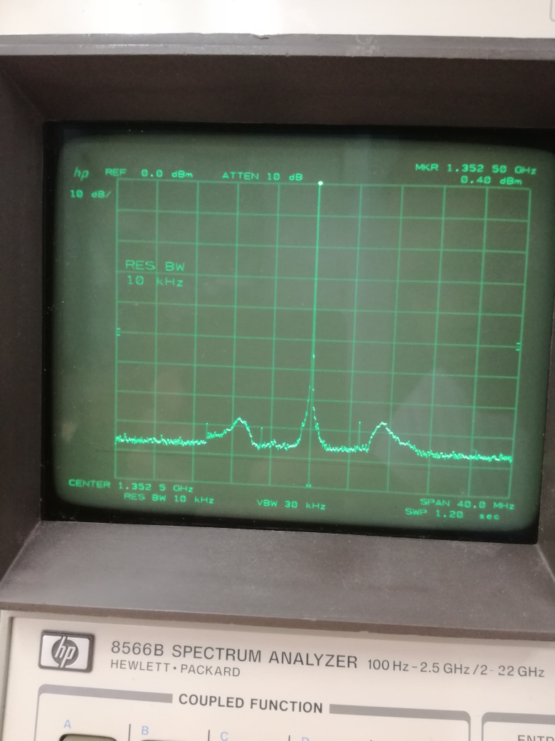
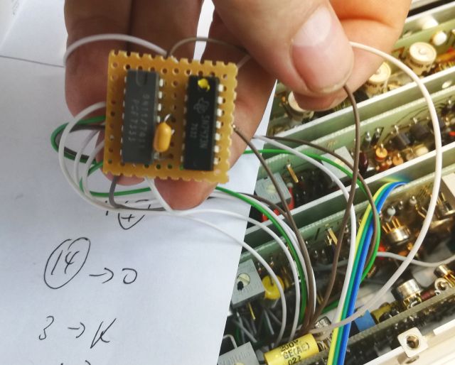
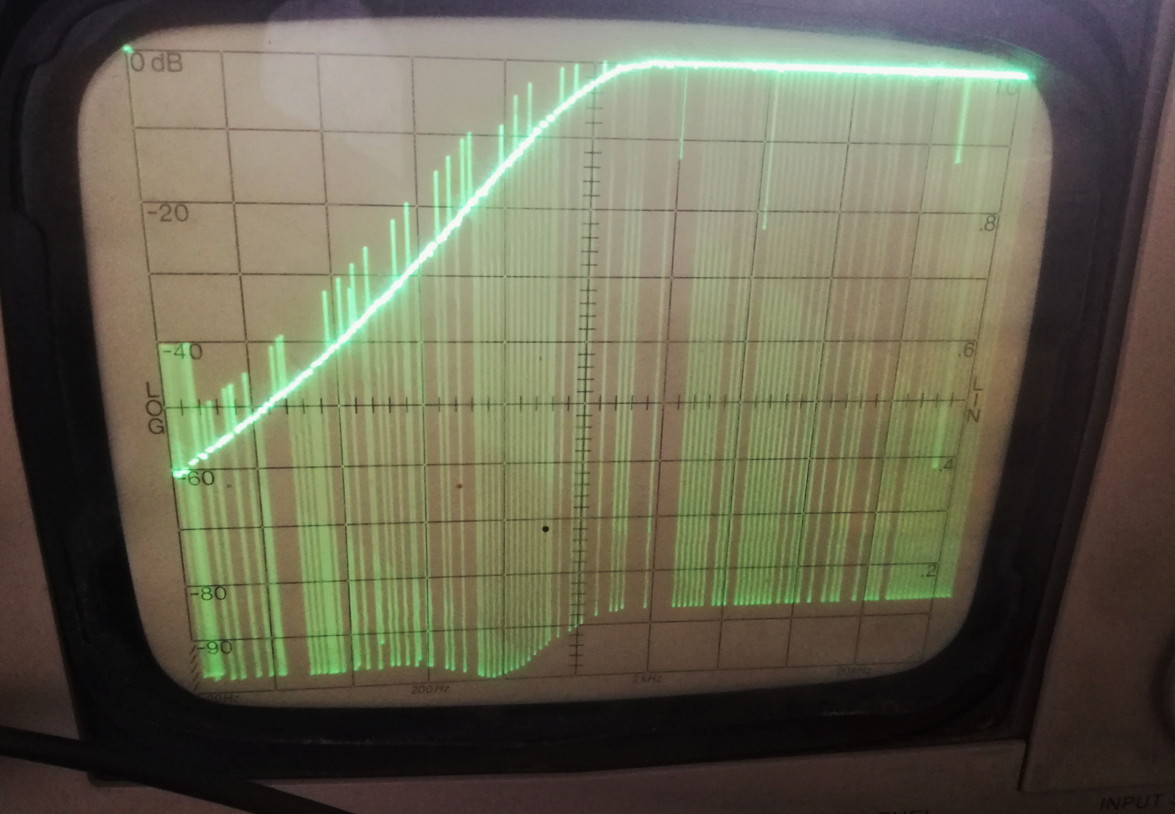
Test 2, now running with a 10 MHz reference clock, and still 26 MHz output to the u-blox M7 (in all cases, the u-Blox has been modified by removing the TCXO, and feeding the clock signal directly to the GPS chip). Sure I known that I am running the Si5351A outside of the specified range – but after all the research, Si5351A Spec, Myth and Truth, I believe this is OK.

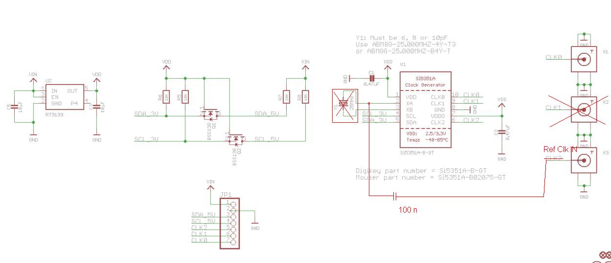
The test setup – note the dotted additions – this will be the later phase locked circuit.

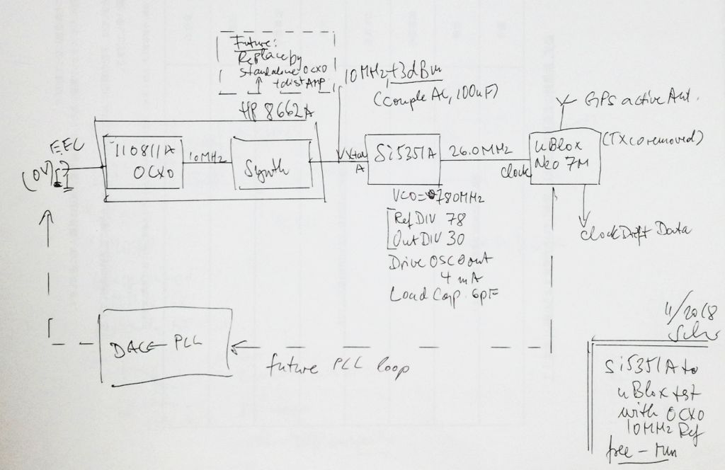
The register settings – running the Si5351A VCO at 780 MHz allows the use of integer-only dividers.
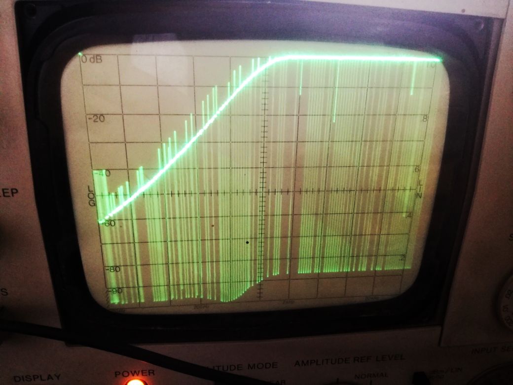
Capacitance set to 4 pF (the lowest value possible for the Si5351A, but it has little effect on sensitivity, 10 pF default setting works as well, maybe 1 dB decreased sensitivity, but we are anyway feeding more then enough power to the Xtal A input of the Si5351A).

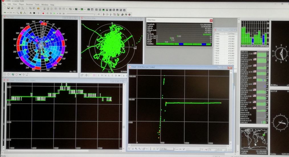
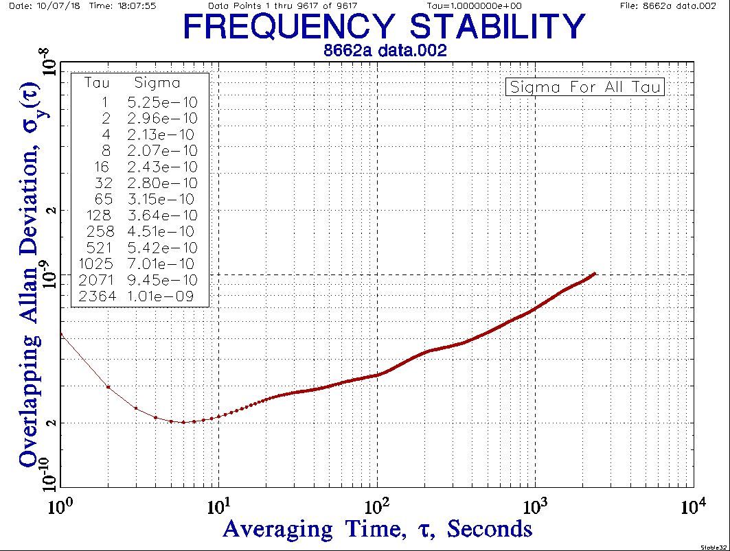
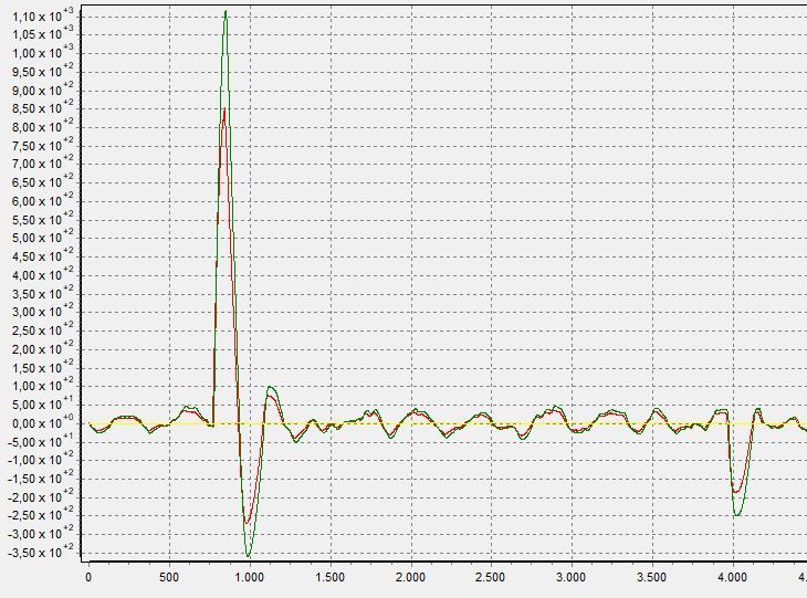
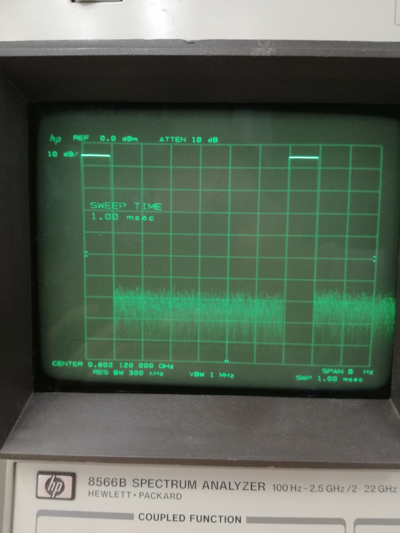
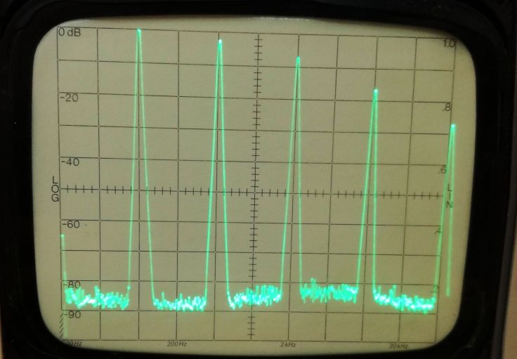
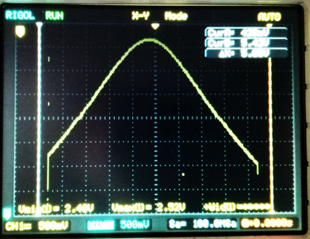
The GPS clock drift data – not very exiting – no drift at all, less than 1 ppb over a few hours. There is a slight frequency offset, because the electronic frequency control (EFC) of the 10811A OCXO set to 0 Volt, rather to the proper value for exactly 10 MHz, only for convenience and to avoid any artifacts from EFC DAC noise or drift.

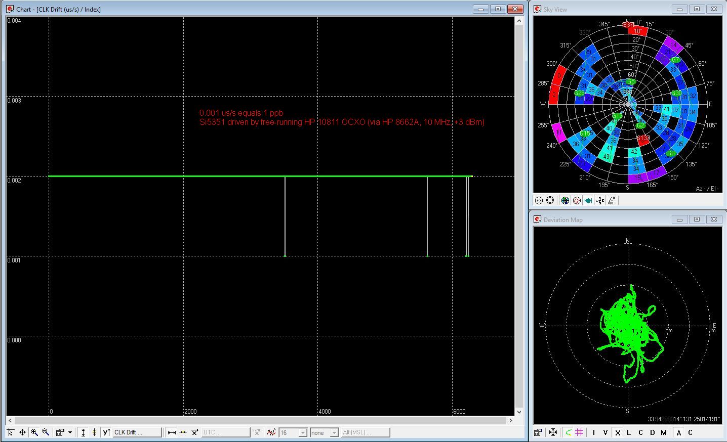
The position accuracy also seems better with the stable oscillator, but may need to check this again after acquiring data for a full day or so.

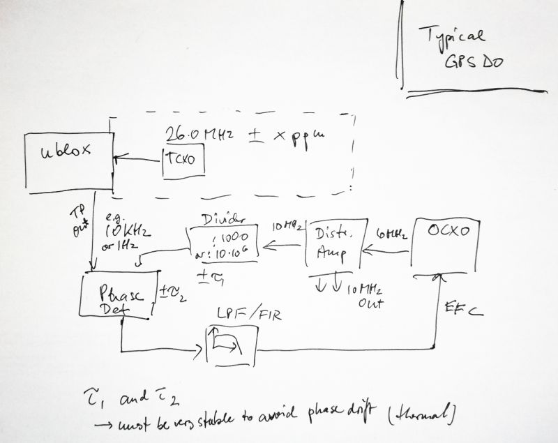
All in all, more than a proof of concept. Next steps include setting up a stand-alone OCXO (I have a couple of spare 10811A OCXOs around), a distribution amplifier (nothing special, planning to use some 74HC14 with small signal transformers for isolation), and getting the PLL code into a microcontroller. For the DAC, I will use a fairly basic model, and provide a low pass filter at the output (much faster than the digitally-generated long time constant low pass of the PLL loop, but still slow compared to common standards) to reduce noise.

So far, the bill of material is very low, just a few dollars, including the GPS receiver. My goal is to stay below USD 10 total, excluding the OCXO, to achieve better than 10-9 stability, and an output with no jitter or other issues.

Si5351A “Any-Frequency CMOS Clock Generator and VCO”: Specifications, Myths, and Truth

The Si5351 series of silicon-VCOs and clock generators is a quite remarkable achievement of technology. Earlier on, we needed two sets of dividers, PLL control logic, and a VCO – essentially a box full of parts – to realize the same purpose: generating one clock, from another.

While being quite adaptable to all kinds of circumstances and uses, the Si5351A (which is the cheapest, and most common chip – all the others have so many pins, and are in such small package that they are hard to use) has some limitations.

(1) It only has a crystal (XTAL) input, specified over a narrow frequency range. 25 to 27 MHz. Some forum comments suggest that there is a tuned oscillator inside, only working at such frequency, Myth or Truth? For my particular application, I need to drive it by a 10 MHz external clock, because that’s the main frequency source and signal I have available.

(2) The VCO range, 600 to 900 MHz should be selected, according to the instructions. Any chance to use lower frequencies, in case this is needed to get integer-only division ratios? Or higher frequencies? What are the limits?

To test the Si5351A, we can use one of the cheap break-out boards. I used the CJMCU-5351. Including SMA connectors, just a few bucks! I can’t really make it any cheaper, and this board also has level translators, and a 3.3 V supply, which is needed because the digital control will be running on good old 5 Volt logic. The I2C control signals are conveniently provided by a Atmel Atmega168PA controller, from a shared 5 Volt I2C bus.

Some modification is necessary – we need to remove the crystal, and add a small SMD capacitor, and a short wire. Once of the outputs, we cut the trace an re-purpose it as an input.

Before modification:

After modification:

The schematic, it is quite similar to the connection method suggested in the Si5351 datasheet.

Datasheet:

Actual modification and test circuit:

Obviously, to test the Si5351 over a range of reference input, we need to set the internal dividers (to lock the VCO to the reference clock input, and to divide it down to a suitable output frequency) to suitable values. Generally, 900 MHz VCO frequency, and 0.5 MHz output frequency has been selected. The low output frequency helps to see any glitches and jitter on my rather moderate scope I am using here (a 60 MHz Tektronix analog scope). At each setting, I increased the reference frequency until the Si5351 lost phase lock. Also, I reduced the power level at each frequency until some jitter showed up in the output.

The tests took more setting than expected – because the Si5351 can handle a huge range of reference frequencies – well beyond the 25 to 27 MHz, and even the internal divider can be set outside of the specified range (necessary only for the highest reference clock frequencies). A particular useful fact – the Si5351A can accept input frequencies of 100 MHz easily – I have some microwave PLLs running of a 100 MHz (rather than 10 MHz) reference.

As you can see, the internal VCO is working from about 170 to about 1100 MHz, so the 600-900 MHz is a good suggestion, but you can also run the VCO at, say, 500 or 550 MHz, if needed in some specific case of division factors (it is always much better to use integer-only divisors, rather than any fractional terms which introduce jitter and spurious signals.

After all this study, we can also plot the input sensitivity (signal from a 50 Ohm source, directly AC coupled to the XTAL A input, XTAL B floating, no other termination – probably, I will measure the characteristic impedance of the input later, no suitable test equipment currently available here in my temporary Japanese workshop).

As you can, see there is no tuned circuit or anything like it, the xtal input can accept any signal up to the highest relevant frequencies, and at lower frequencies, you just have to drive it a bit harder. 10 MHz may be the useful low limit (I suggest you drive it at 3-5 dBm when using 10 MHz, which will be about 6 dB above the sensitivity threshold).

Now, up for some long term test in the actual GPSDO application!

Agilent 4352B VCO/PLL Signal Analyzer: a great find (hopefully!)

I found a great deal on a “totally faulty” 4352B, well, it is a bit a cat in a sack, as we say in Germany, you never know what you get. It shipped from Manila, even better! List price, I think it was close to USD 50k!

It’s a clean unit, except for about 100 stickers and seals!

All heavily shielded, many kinds of screws and metal plates to keep to good waves in, and the bad waves out.

The brain of the machine – quite sophisticated – Japanese engineering (this unit has been manufactured by HP Japan!).

After some study and test, it is clear, it is dead because there just isn’t any power. The power supply is a two-stage supply, first stage, a switchmode universal voltage to 24 Volt (190 Watt) supply, bz maker Artesyn, then a really top quality 2nd stage, made by Agilent. And guess what, the 24 Volt supply is faultly!

This supply uses power factor correction, and two IRFBE30 MOSFETs to drive the transformer – one of them is shorted shot. Otherwise, no damage to be found on the board so far, except the thermal fuse, which must have cut out immediately (even the primary fuse is OK – so there is hope that this will be an easy repair of the 24 V supply).

Ordered some spare thermal fuses and MOSFETs, quite common IRFBE30 type – low cost. Let’s see if this will let us get the power back, if not, worst case, we can always install a new 24 V 200 W supply – there is enough space in the case.

In any case, these VCO analyzers are a great deal – there is a 26.5 GHz (!! APC 3.5 !!) power splitter inside, value, still available today, EUR 1350, and a 13 GHz detector, value, 450 EUR. But let’s keep fingers crossed that this won’t become a parts unit anytime soon.

The 08662-60001 low noise VCO: the heart of the HP 8662A

This is certainly one of the electronic antiques and marvels, which had the most hidden and non-spectacular impact on mankind and development of mobile communications in the 80s and 90s – the VCO of the 8662A/8663A, the defacto standard for low close-in phase noise signal generators.

The concept, it is a switch reactance oscillator, i.e., the inductances will be switched, to cover the 320 to 640 MHz range, rather than doing this all by varactor diode tuning.

For low phase noise, you need an oscillator with high Q – this is achieved by strongly biasing the varactor diode over the full tuning range, and by low resistance PIN diodes (two in parallel, see below!), that switch the thin-film inductances embedded between lexane disks.

Note the small indent on the golden patch on the PCB? This is where the copper bolt reaches in to adjust the frequency offset.

All this is housed in extruded aluminum, end a layer of special steel which absorbs magnetic fields. So far, I never had the chance to look inside of these – but a kind reader this block, Martin, shared this picture and I put it up here for those interested.

The designer of this marvelous and magic device, his name, Dieter Scherer, a German fellow of HP, unfortunately, I have never met him and don’t know if he is still alive. Sure he left behind great achievement and a legacy of high frequency engineering.

u-blox GPSDO: Update!

With the hardware already set up to provide a 10 MHz signal and electronic frequency correction, some optimization of the algorithm used for phase locking. It needs to be a really low frequency low pass filter (say, 0.001 Hz), and we need to deal with the discrete nature of the measurements and the quantization.
This is accomplished by three mathematical approaches
(1) The data is sent through a 32-parameter FIR low pass.
(2) The frequency drift is calculated for the last 32 seconds, and used as derivative signal, as long as the oscillator drift is less than 10e-9 (1 ns every second!).

The u-blox settings – these are no timing receivers, but I set the device for 2D stationary navigation, it gave the best results here. Also, better disable all messages you don’t need, it will be beneficial to avoid overloading of the slow serial interface (still running at 9600 baud).

Here some examples:

With the PLL open, the signal is drifting away, albeit, at a very small rate.

To check the stability and general behavior, I’m monitoring the 10 MHz signal on a scope, triggered by the time pulse (set to 100 kHz) of a 2nd u-blox receiver, sitting closeby. Horizontal deflection is 10 ns per div. Sure, the signal is broadened by the interpolation of the 2nd receiver, which has a free-running TCXO. Because of the synthesis of the 100 kHz signal from the internal 48 MHz, the trigger has about 20 ns jitter-no problem here, because the drift is much stronger and the phase of the 10 MHz signal relative to the 2nd receiver can easily be measured down to 1-2 ns.

u-blox GPS receiver: a self-regulating clock, and a GPSDO, and all of this, for the lowest cost

The quest for precise timing, it is a mainstay topic for all serious electronic enthusiasts, and for a good reason – it offers so much insights into receivers, oscillators, phase detectors, regulation theory. After mastering such design, the hobbyist has himself earned a masters (or at least bachelor’s) degree.

With the advent of compact and really powderful GPS receivers, like the u-blox devices, receiving GPS signals is no problem any more, and in fact, it has never been over the last 20 years, with various Motorola receivers, etc.

The u-blox devices have a feature that makes a reference frequency (derived from its internal 48 MHz clock) directly available, rather than just the 1 pps signal that is not all that easy to use for locking a 10 MHz reference to it. The u-blox signal, which can provide a jittery 10 MHz, or, preferably, integer-divided 48 MHz (e.g., 8 or 4 or 2 MHz), has been widely used as a reference frequency in the amateur world, and u-blox company and other recommend to use an external PLL to clean up the signal according to below scheme. This implies that the GPS will be running on a drifting local osciallator, and with a good amount of knowledge and software u-blox is mastering the drift prediction and corrections, and after all such effort an external oscillator, typically, an OCXO is kept in sync with the GPS true clock, by even more phase detectors and control loops. It is doable, logical, practical, but not very clever.

Sure there a better and much more expensive GPS receivers, and even special timing-related u-blox devices (about 10x more expensive than the regular receivers), which can control an internal VTCXO (voltage-controlled temperature compensated local oscillator). With such approach, the drift of the local osciallator will be small, and all in sync with the GPS frequency, but still, it is not as precise as a really good metrology grade OCXO. I am still relying on some well aged HP 10811A oscillators.

That’s the magic neo-7m device, or a Chinese copy of it, you never know – but all that really counts is good reception, and this can be easily checked.

Which secrets hide inside the metal can? Well, let’s find out. Most important part, the G7020-KT GPS processor, it is a remarkable piece of engineering, and u-blox must have a crew of the most well educated, highly paid and hard working people to come up with such devices. Also, they know that they must protect their inventions, and even the datasheet of this device is strictly confidential, although you can find it at many places. What you can’t find are some secret control codes that would allow us to use a 10 MHz clock directly as the clock source for this chip – it is running on 26 MHz by default, for whatever reason! Internally, the other frequencies are synthesized from this 26 MHz anyway.

The typical TCXO performance, it is not bad, drifting along, and we can do some further stability analysis on it. For such a small thermal mass, the performance appears quite good. Accurate to 0.5 ppm over temperature, and 1 ppm per year.

That’s the GPS with the TCXO…

With no effort, the TCXO can be removed, just by holding a soldering iron to it to heat it up.

After removing it, we just solder a thin RF cable in position. In my temporary workshop here, I don’t have better tools, so this must work for now. Ideally, you add a decoupling cap, and solder a wire to a solder post or other propper connection or contact.

We have no good information what level of power is needed at this input, ideally, a 0.8 V p-p min. signal, DC coupled, but we don’t have such signal generator here, only a HP 8662A, which has sinewave output. Using the u-center software, and experimenting, the receiver works well from about -5 dBm of coupled power at the clock input. Operating at 0 dbm, that’s enough, we don’t want to fry this chip.

Even with a small antenna, good reception, within the (wooden) Japanese house.

Now, the feature we are going to use – not the reference frequency output of the u-blox, but the UBX NAV-CLOCK message, which is no less than a phase detector and drift measurement device, of the clock signal, relative to the GPS true-software-reconstructed clock. Marvelous.

As the new 26.0000000 MHz source, we use a 8662A generator with HP 10811A reference, and an EFC (analog frequency control input, about 0.1 Hz per Volt). On top, a 35601A interface, only using the DAC portion of it to generate a tuning voltage from the host computer (connected via GPIB). It is not the most handy DAC, but the only one I have around at the moment.

First, we try without any feedback – Allen deviation. First, the plot using the original TCXO, next, the same receiver (at the same location and setting), with the 8662A (freerunning).

The 8662a – not yet fully warmed up, but already one decade better – or even more, because of the resultion of the phase detector (1 ns!).

Next, we need to do some programming – this will later be put into a microcontroller, but for now, we use a regular PC, running a C program. This program reads the NAV-CLOCK message from the u-blox receiver, does a magic calculation, and then sets the EFC voltage of the OCXO, which in turn determines the 26.000 MHz clock for the same u-blox receiver. And after not too long time, all is frequency looked.

Here, some first results (using a rather small bandwidth regulation loop, just to proof the principle without waiting for too long time).

Introduced some artificial disturbaces, and the system is reacting well.

Next – using a Silicon Labs clock generator, and a stand-alone OCXO to do the same thing, and then, the software needs to be put in a small microcontroller (currently running a rather calculation intensive floating point algorithm). Stay tuned.

Micro-Tel SG-811 Signal Generator: a second unit

By luck and coincidence, I found another Micro-tel SG-811 generator on eBay, at a very reasonable price – sold as not working. Even non-working, these units are great because of the many microwave components contained: YIGs, filters, GHz-capable relais, SMA cables… and a lot of old-fashioned analog circuits.

First check – the fuse! Someone recklessly put a 10 Amp fuse in, because the smaller fuses would blow. That’s never a good idea. Most probably we will have to deal with a power supply repair.

After detail assessment – the 24 V tantalum cap is shorted, maybe this triggered a sequence of faults: the main primary transistors (MJ12002), the rectifier, and two thermistors that limit the inrush current.

Micro-tel didnt safe on screws when they designed the power supply!!

These power thermistors are hard to get – I just desoldered two similar ones from old switchmode power supplies.

A dead rectifier – easily fixed.

All the parts labeled – also replaced the 2N2222 driver transistors, and two tantalum caps that were leaking current.

The most precious parts – the RF section.

A most complicated arrangement of oscillators, switches, couplers, and so on

Some of the oscillators originally used in these units required a variable supply voltage to get stable power output, but strangely enough, the YIG oscillators fitted have built-in voltage regulators, and the supply voltage has no effect at all on their output. Still, the power supply board caused issues – end even overheated, because the voltage is set by very sensitive trimmers, and drifted above 18 Volt…

The YTO has a voltage protection diode – it was completely fried when I received the unit. Checked some good Advantek YTOs, these have 18 V 1.3 W Zeners for voltage protection.

With power back on, and the voltage at the YTOs OK, still no good output – how can it be? Some issues with the oscillator driver board that sets the current of the main coil, and without a proper magnetic field, there won’t be any oscillation.

The precision resistors, seems they were hand soldered with some bad solder (traces of corrosion, and high melting point).

First, some trouble to find the dead part – thought it is one of the opamps, LM308, replaced it with a OP02. But no luck.

So I changed it back to the old LM308, just to keep all in original state.

The bad guy… a 4051 multiplexer CMOS, these are notorious!

Another interesting assembly, the reference assy – the 1N 827 reference diodes where still very accurately set, only a few ppm of the 11.000 V, and -11.000 V!

After these repairs, and some adjustment, all is back to working condition!

Checking out the signal on a 8566B analyzer. All good!

The pulse generator, also a great feature of this unit… 1 ms pulse.

down to 1 microsecond, no problem.

… 10 microsecond pulse…

The attenuator, a really high quality HP device.

The manual has some remarkable comments – use a 2 kbyte memory, just in case a “really big program” would be needed in the future.

Still, I will do some alignment of the oscillators and filters… but that’s no big deal.

HP 3580A Spectrum Analyzer: Digital display fix, and ancient CMOS circuits

With most of the 3580A functions working again, we still need to fix the digital display. Essentially, the 3580A uses a digital scope circuit, similar to those use in digital oscilloscopes of the 70s.

First, some study of the ADC. The 1973 HP Journal has all the details, it is successive approximation, peak detecting ADC.

Checking the input to the digital display board, blue trace, and the comparator/approximator input to the ADC, yellow. Seems something is wrong with the ADC ciruit, or it’s timing-counter control systems.

After considerable checking and probing, I found the issue, a dead 4019 CMOS, 4×2 multiplexer. Replaced it with a “new” part, taking great care to avoid any static discharge to the board.

The dead part, it is almost a historic piece! 1974, only a few year after the introduction of CMOS circuits by RCA!

That’s the full board. Multiplayer construction. Plenty of precision resistors that are needed for the ADC circuit.

Another working antique part – the 2102 S-RAM, Intel, 1 kbit per circuit. 8 pieces – a total of 1 kbyte of SRAM!

Working display…

10 kHz reference display… Great!

Even the log scale scan is working.

One tip – put all the screws and parts in a box, and check that it is empty afterwards. So many instrumented I receive here in the workshop are missing some screws or other parts.

HP 3580A Spectrum Analyzer: a few mechanical repairs, and sweep test

With the basic functions of the 3580A restored (at least, it is sweeping again), some attention needs to be paid to the mechanics. Fortunately, all is good with the intricate tuning assembly and digital display, but the knobs have some cracks, probably, a combination of age and stress.

Everything taped up, and the cracks filled with rapid-set epoxy resin.

To apply the resin to the small cracks, you can use a piece of stiff plastic foil, cut to a tool of appropriate size –

Here, a few close-ups of the tuning mechanism. It has fast tuning, and fine tuning, a clutch, several gears – all good old analog technology.

Finally, some test of the sweep circuit – but how to test a 200 second per division (i.e. 2000 second per screen) deflection for accuracy and linearity? Well, I connected it to a 34401a multimeter, and recorded the values for several hours by GPIB interface.

As you can see, the sweep is very linear, only some minor deviation at low voltages (maybe connected to some offset voltages or similar effects of the operational amplifier), at least, we can’t see any leakage current of the capacitor, which would show up as increasing sweep time with higher voltage/later divisions.

Also interesting, see the accuracy of the sweep speed, with warm-up of the instrument (each measurement is 2000 second). Still, after all these years, well within the 5% specification of the sweep time! Amazing!

HP 3580A Spectrum Analyzer: a non-working marvel of engineering

The 3580A is a audio spectrum analyzer of the 1970s, and not only useful for audio, but anything that can be converted to audio frequencies (e.g., noise analysis of GHz sources, provided, you use the appropriate mixers). This marvel is not a FFT machine, but a discrete audio “received”, using a low-noise local oscillator, and covering a frequency range from 5 Hz to 50 kHz. The resolution filters are quarz filters, with bandwidth down to 1 Hz! Dynamic range is over 80 dB.

The device, it comes from my old university, and has been sitting there on the shelf for a while, not working. And in fact, it shows not many signs of life, it is not sweeping properly, and even in manual mode, it is not working reliably (not showing any reasonable signal, but there is some activity on the tracking output which suggests that the instrument is not all dead, also the “overrange” LED is working).

After some study and test it became clear the the issue is with the ramp generator. Unfortunately, it is not a simple ramp generator, as you can see below.

The main circuit is a capacitor being charged by a current source (mechanical switch with resistors).

The voltage at the main capacitor, a 10 µF polyester hermetic cap (really high end with glass seal and metal case), is charged and its voltage amplified by a FET-opamp (the FET input constructed from a discrete FET pair, and a PTFE stand-off to keep this all really high impedance).

All the sweeting action is controlled by a state controller, more or less, a hardwired program with several TTL chips. It took me quite some study to understand how it is supposed to work. But fact is, it doesn’t. Clearly, the issue is with the A3 assembly. This must have been quit an expensive assembly at the time, with all the FET pairs and opamps. Still today, not an easy thing to fix.

At least, it is a beautifully arranged board, all gold plated and really smells like quality. So it is worth some time and effort to fix it.

Key for such repair, at least in any reasonable time, are a set of good schematics. Fortunately, I have a set around and printed out really large copies – it is worth the effort, because without making some notes, you will struggle to keep all in your brain and still work on the circuit.

With no extender board available, just soldered some wires to the board to monitor the state of the main state counter, and some of its inputs.

Hmmm, after a lot of probing, I was almost tempted to replace a good part of the TTL chips, because it is really hard to find the defect in such a complicated and loop-wired logic circuit, including its analog parts.

But after a bit more consideration and test, I decided to try a step-wise approach, starting from the most likely parts causing issues. One of the 7473 dead, no problem, there are spares around. But the next one – a 7472! This is an AND gated J-K flip flop, with three inputs to each AND gate… in simple words, something old, exotic, and rarely used. Went through all my piles of old boards and ICs, but no 7472 to be found! Quickly arranged a temporary 7472 – from a 7411 3-input AND gate and a 7473 flip-flop.

To be sure, I tested to old 7472 – indeed, it is not working.

With the A3 board temporary fix, a quick test of the unit.

Unfortunately, still some issues, but is is sweeping:

Display issue:

Check with a X-Y scope (on the rear outputs of the 3580A) – all seems good from the analyzer section, maybe some issue with the storage display?

Finally, on xbay, found a set of 5 pcs 7472 at a reasonable price, from Spain! NOS (=new old stock), about the same age as the 3580a!

Some fluxing issue with the soldering of the old ICs (clearly seen at the 7473), beware! Use some good flux, or solder from both sides.

SimonsDialogs – A wild collection of random thoughts, observations and learnings. Presented by Simon.