HP 5086-7803 YIG tuned Filter and Switch: “SYTF” details and adjustment

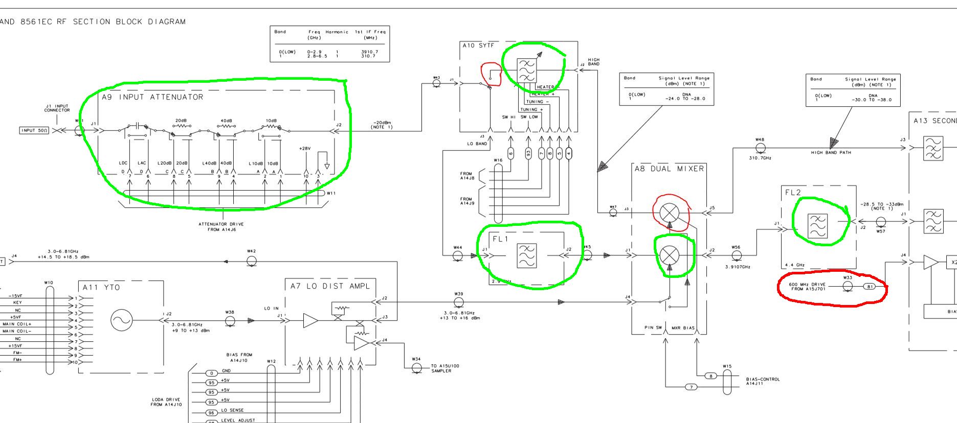
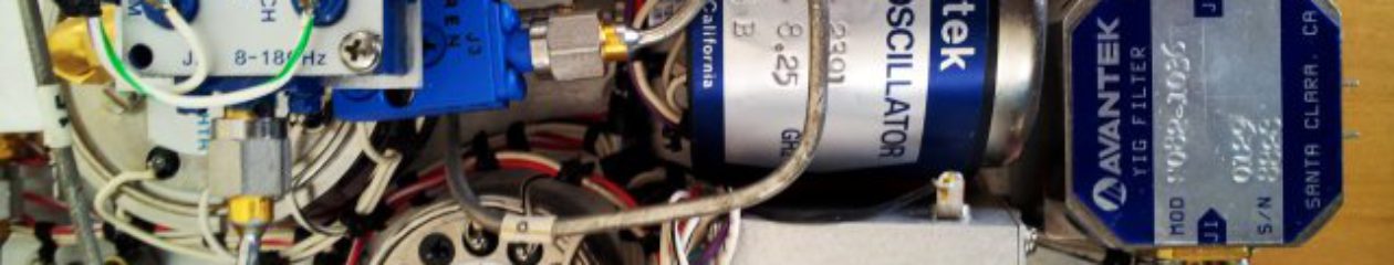
With the repair of many spectrum analyzers, it turns out, the preselectors are usually not easily damaged, because of their self limiting characteristics, and because of the absence of active parts. The SYTF is diffient in that it has an active part, a switch.

It is already some years old, but no reason why such parts should have much aging at all.

The symptom of this unit, it is working in the low frequency region setting, LOW band out, but the high band is dead, loss in excess of 35 dB, at all frequencies, and independent of the tuning current supplied.

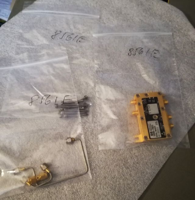
So my first assessment was, this unit needs replacing, and I found a replacement part online, from a US seller, not cheap, but OK, the 8561E analyzer is worth it, if it is working again after the repair. Unfortunately, several week of waiting were all for nothing – the seller shipped the wrong part and it took a while to get the money back, but finally all settled, except, we still have the defective filter.

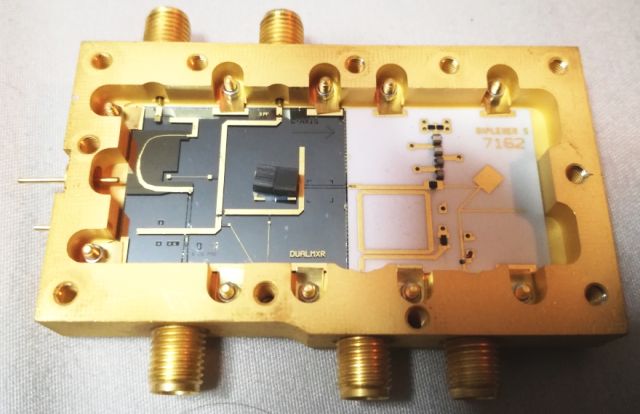
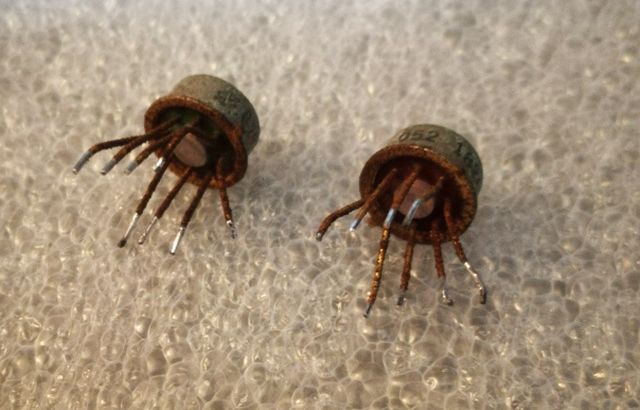
Let’s try to investigate the nature of the defect, and open it up. Fortunately, these filters are not hermetically welded like some other YIG parts.

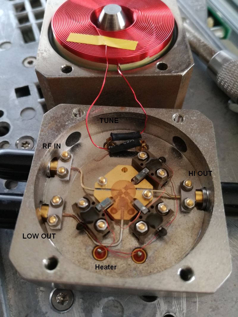
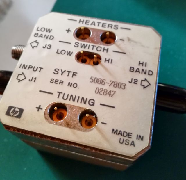
You can clearly see the coil, the inlet and outlets (low and high band) by rigid SMA cable (1 mm size!).

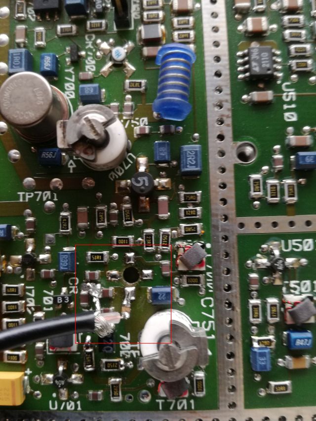
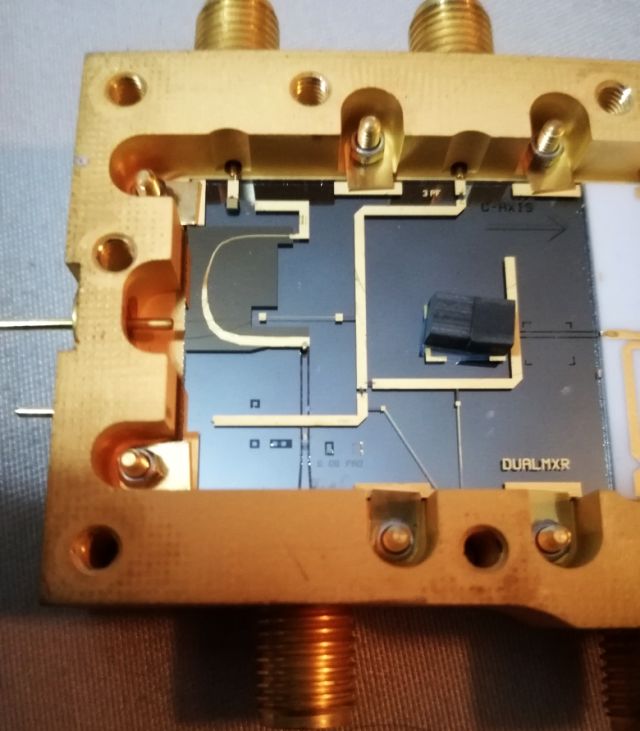
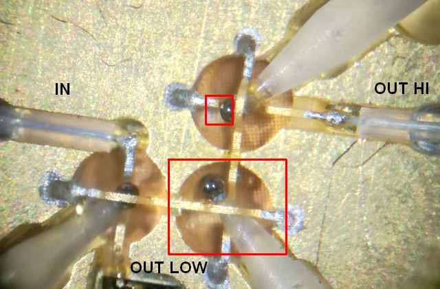
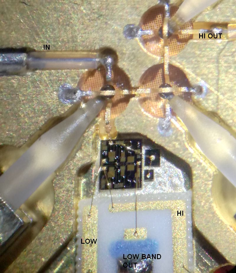
First, let’s study the switch. It is not actually switching the high band, as I originally assumed, but it is switching on and off the low band.

It is a series-shunt-series type FET switch, controlled by about -10 V negative voltage (1 kOHM vs. -15 V connection is the usual control method, floating or ground to switch off).

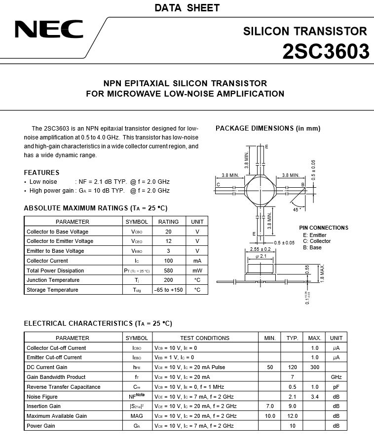
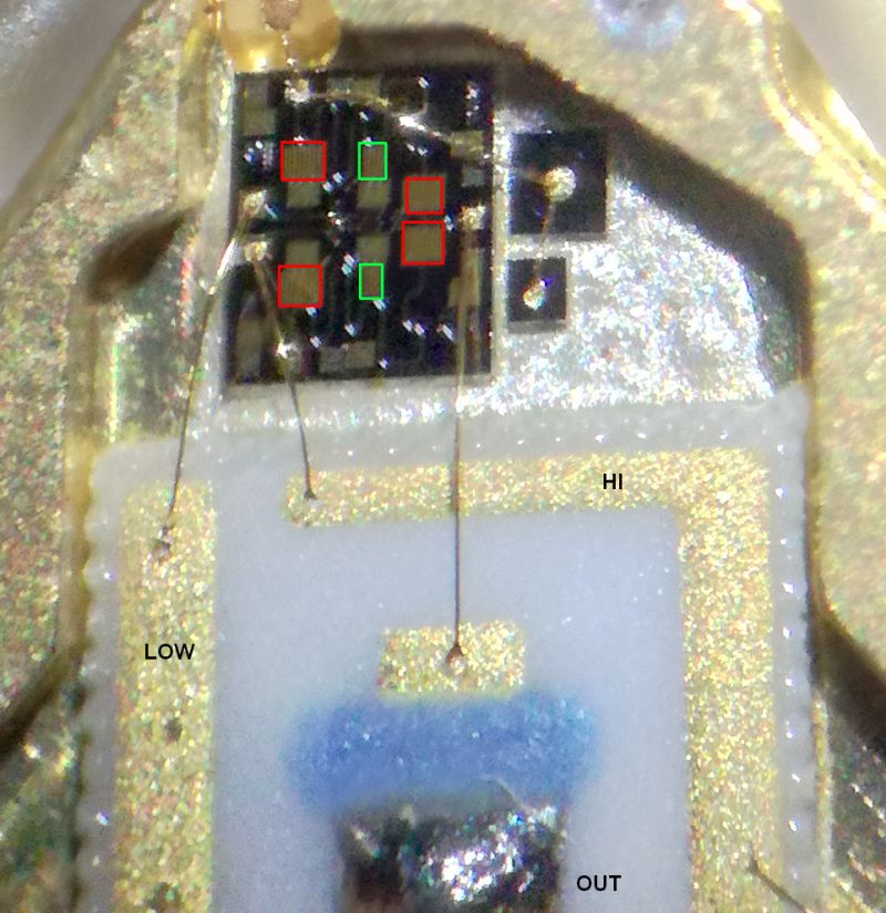
I could not find the exact die and model for this switch, but there are many similar models that clearly show the structure. The shunt and double series construction will provide very high isolation.

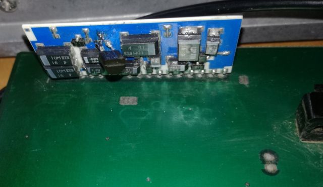
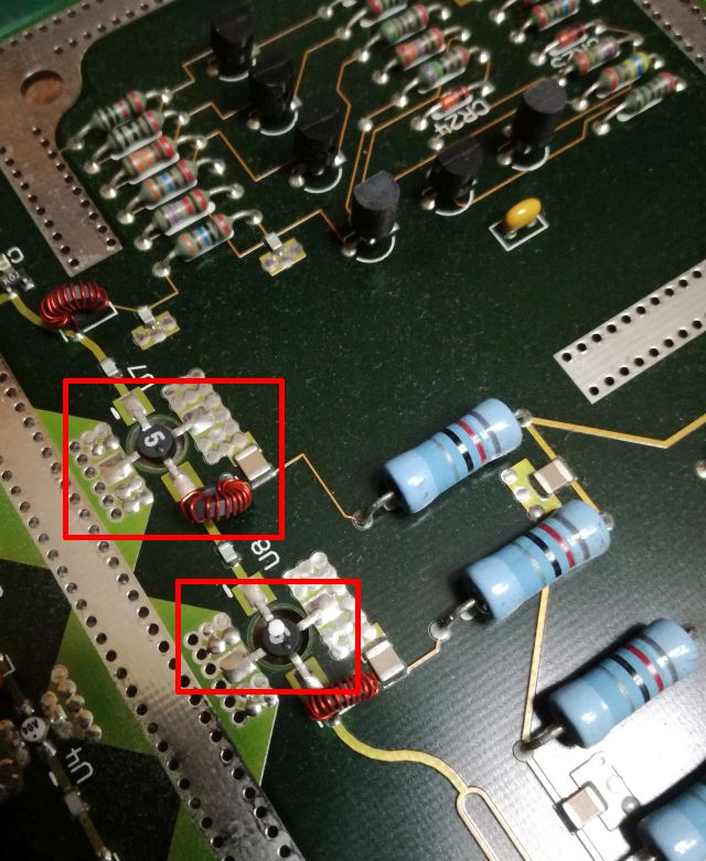
After removing carefully the gold mesh (it is only lightly glued on, I will use some tiny traces of epoxy to stick it back on), some study under the microscope.

Clearly, the spheres are misaligned! The spheres must be placed in the center of the coupling loop, to allow for RF to couple. Generally speaking, during alignment, the sphere is only turned, and then the position fixed by some epoxy – which all seems to be intact, and solidly fixed. So what has happended? I think it has to do with the mounting blocks, which are of different material compared to the based (which needs to be magnetic Fe-Nickel alloy). With frequent temperature cycling, I believe there is some migration of the mounting blocks, fractions of a micrometer every time (keep in mind, the YIG spheres are heated during operation). While we can speculate about the reason of the migration, the result is clear, and the action as well: we need to realign the spheres.

I decided not to undo the screws because the coupling loops can be easily damaged, and used a screwdriver to carefully push the mounting blocks away from the coupling section, bit by bit, under control with a microscope.

Finally managed to get all the sphere properly aligned. If you don’t know how it works, never turn the YIG spheres! These need to be aligned for thermal stability effects, not only amplitude – something which you may have trouble doing at home.

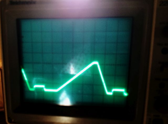
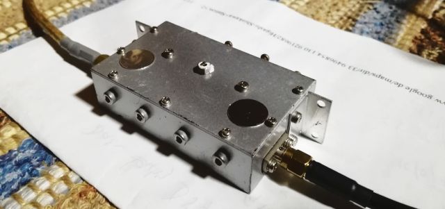
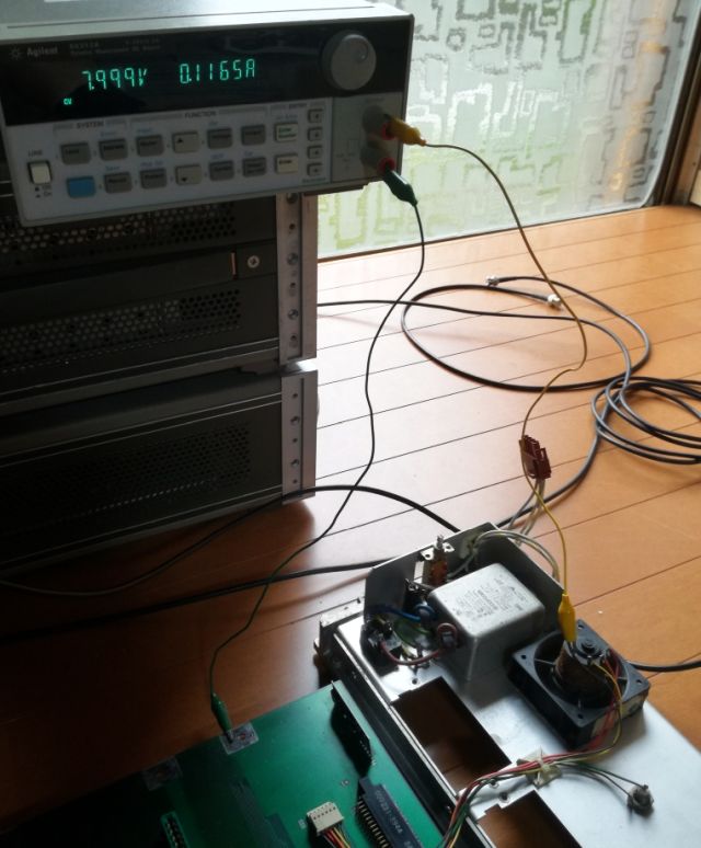
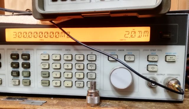
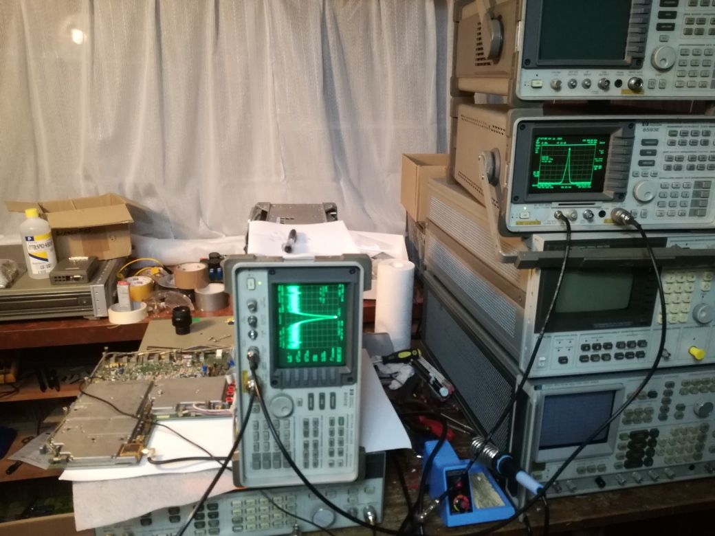
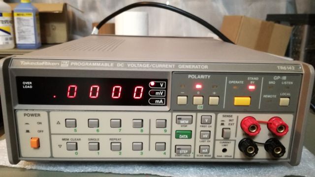
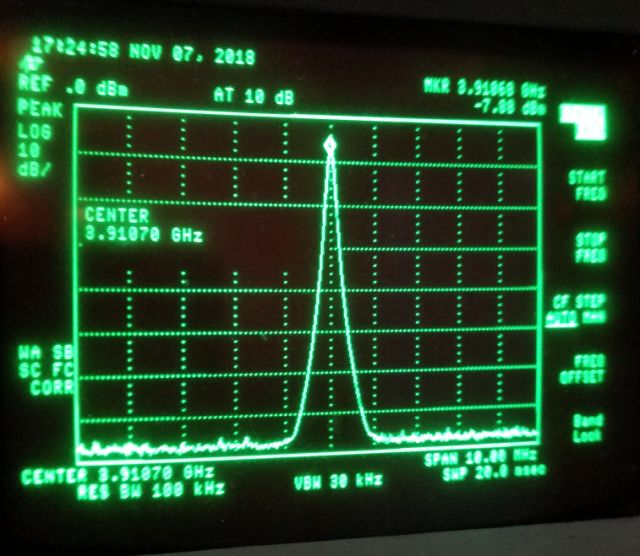
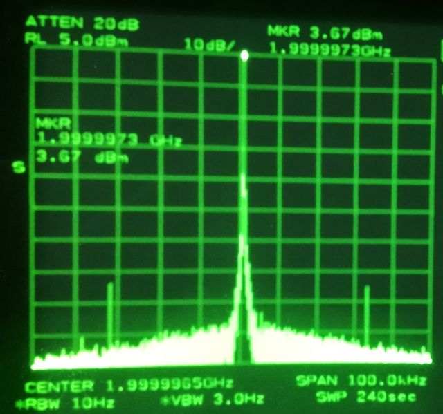
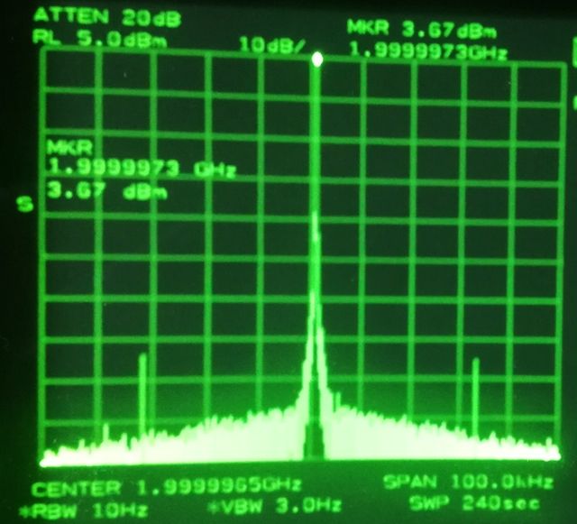
After all the alignment, a quick test setup, with a current source for the main coil, and another supply for the heater and switch connection. Note that the current source is set in parallel with a capacitor (22 uF) to allow for stable regulation with the strongly inductive load.

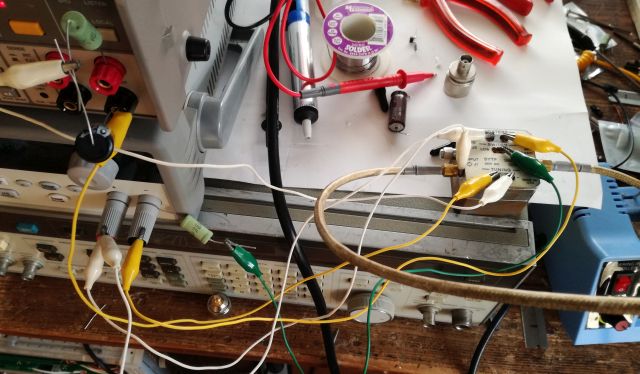
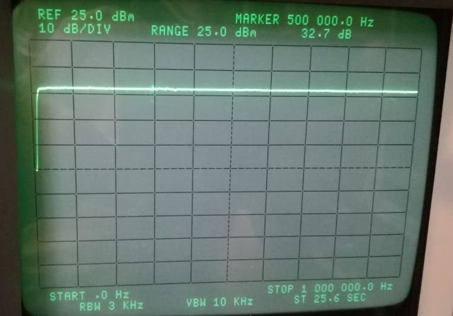
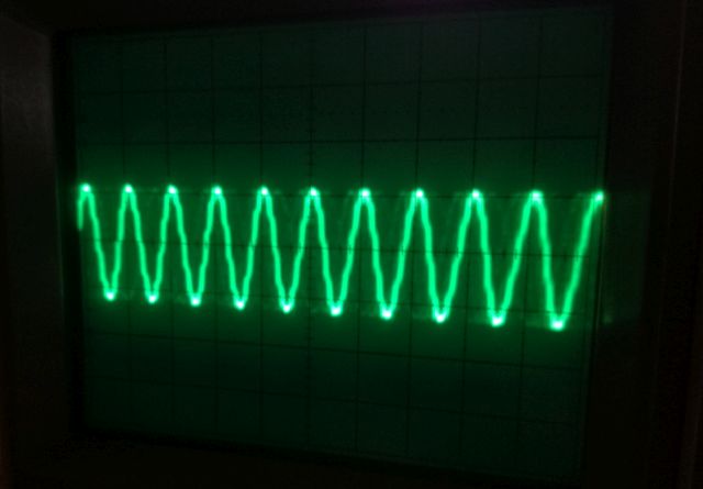
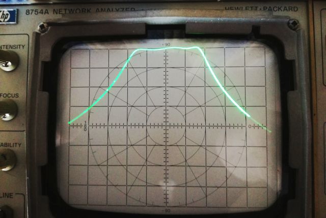
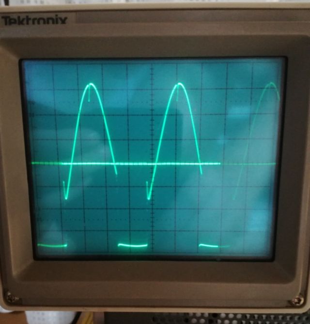
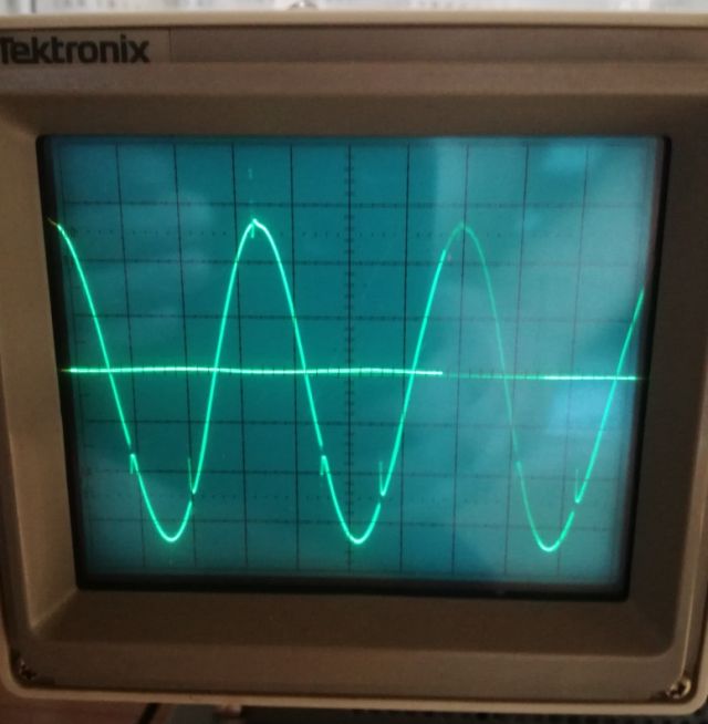
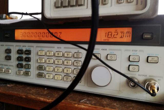
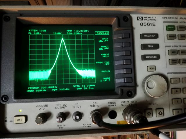
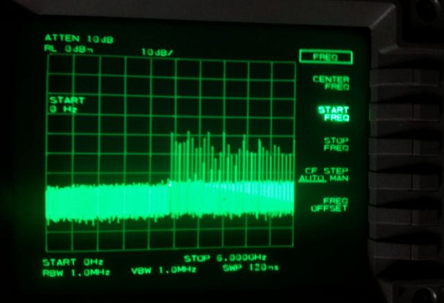
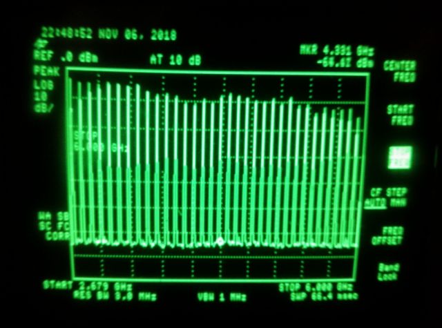
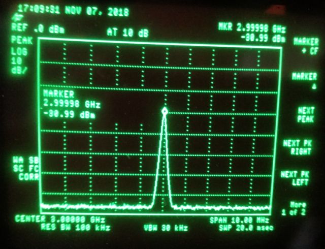
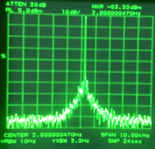
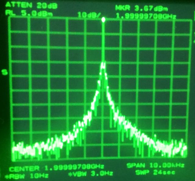
The insertion loss test – done by checking at several frequencies, using the lines of a good comb generator.

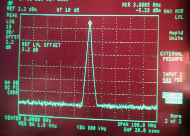
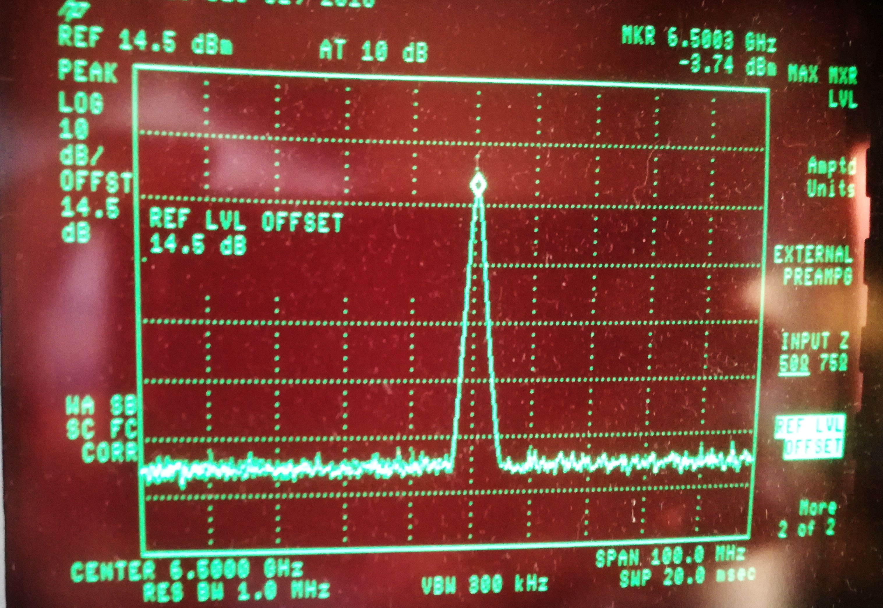
The insertion loss, in my simple setup, it is about 4-6 dB for a 3 stage filter, not bad. I don’t know the original performance spec, but it is definitely in the typical range of such filters, and good enough for a spectrum analyzer in any case (in the worst case, we will loose 1-2 dB of sensitivity). Maybe I will eventually find a new filter at a reasonable price, to check it – it could also have moved spheres.

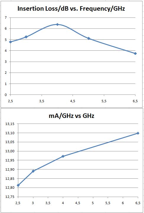
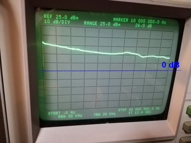
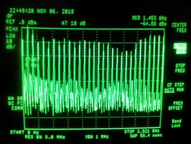
The tuning current is very linear, I don’t expect any issues with using this part in the analyzer (the tuning characteristics can be programmed and stored in the EEPROM of the analyzer, to control its DAC appropriately, also, we will need to recalibrate the flatness).

HP 8754A 4 MHz to 1300 MHz Network Analyzer: an analog computer, and a few rusted transistors

There is no specific need for a 1.3 GHz Network Analyzer in my workshop, because there are already several more modern instruments, but this HP 8754A is a real marvel, it was original designed as a “moderately priced, compact” type network analyzer, whatever was considered moderate by HP at the time (maybe the value of two or three small cars?). Finding the offer for a rediculouly low price, for a non-working unit, on Yahoo Japan, I could not resist to place a very moderate bid. Turns out, I was to only bidder, in whole Japan. My original thought was to use it for some experiments, and then, use it a as a source of HP spare parts (there are many FETs, Opamps, transitors, etc. in this machine).

Once the unit arrived, I powered it up, only to find out two things – the -10 Volt and +5 Volt power supplies are not working. And the CRT is very good and sharp. Maybe not many hours of use. Also, the unit is generally clean and in original condition – no other repair attemped. Even the HP instrument feet were included.

The -10 Volt, it required some troubleshooting of the low voltage assembly (corroded transistor legs), see below. The +5 supply, the issue could be traced to a defective TO-3 HP 1820-0430 integrated regulator, alias LM309K.

This regulator is mounted on an aluminum plate in the chassis, with some rather thick ceramic insulator, and what appeared to be only traced of thermal grease. Usually, these are protected against short and overheating, maybe, it was just running a bit hot for year, eventually, accelerating aging and finally triggering natural/random failure with no external even. We will never know, we only know, we have to fix it.

The LM309K tends to become rare and expensive, I still have some back at the Ludwigshafen, Germany workshop, but not here in my temporary Japanese workshop. Checking the offers, I found some very inexpensive LM323K.

The LM323K, it is a very similar device – just higher current capability. It is not critical for the 8754A, the 5 V rail is only loaded by about 0.25-0.3 Amp (as checked with a power supply).

Now, to the corroded transistors. This only seems to affect the boards thats are close to the air inlet, maybe some contamination from ambient air (salt?) is accelerating the effect, related to gold plated steel wire leg transistor. Other transistors have copper, or special alloy wire, but especially the “4-404” and 2N2222A transistors used by HP in the late 1970s seems to be affected by this phenomenon. Not so much in dry countries, but in instruments subject to humind and salty (sea?) conditions here in Japan – just a few km from the cost in most cases.

The 4-404 transistor, alias SS9333, 1854-0404 HP part number, it is a kind of mystery, no data available, and I have seen this part in may Hp instruments, always replacing them with some 4-404 scavenged from part units, etc. But for the 8754A, should we really buy some expensive old HP parts or wait for a long time to go back to Germany to the parts storage? Time for some characterization – found one good, only slightly rusted 4-404, and did some gain, DC performance and frequency response tests at typical currents.

Some basic data could be found – nothing special, the voltage rating rather moderate, and power rating, as well.

Some tests and calculations, it is medium to high gain NPN transistor. BC337-25 or BC337-40 can be valid replacments, I used BC337-25, selected for a gain of 250-300.

High frequency performance is nothing special, it can be easily met by a BC337.

Several 2N2222A are a bit easier to replace – just replaced the TO-18 metal can units with some generic TO-92 2N2222A (or whatever silicon fragments the mass producers put into the 2N2222A case nowadays).

After these initial fixes, the power is up, and the transistors all good. Initial assessment –
(1) front panel “analog computer” is working, some contact cleaner will do the trick, there is no mechanical damage
(2) the CRT will need a filter, it is missing.
(3) the RF output seems to work, at least there is power – need to check with a counter and properly align the linearity, etc.
(4) The VCO and PLL of the receivers seems to have some trouble, but the samplers are working! That’s a relieve.

See below this is a 35 MHz input signal, sampled with the VCO at about 33 MHz, giving a 1 MHz frequency.

So, what is wrong with the PLL? The PLL, it’s purpose is to have a line of a comb generator/multiplier (which is generating the sampler pulses by a step recovery diode) always 1 MHz away from the RF, to give a 1 MHz IF for the R, A and B channels.

This is achieved by first pretuning the VCO, by setting a frequency close to the needed multiple of the VCO, then the PLL is activated and phase lock achieved.

The phase detector, first, I thought is not working, because there is no proper output. But once desoldered, all the transistors tested OK.

The pretune, also this seems to be working, but hold – it is working too well! It is overruling the phase detector.

Further study shows that there are FET switched controlled by a logic signal, via a LM339 comparator. And, as it turns out, the LM339 is dead (both switches on)…

Temporarily fixed the issue by disabling the pre-tune, and enabling the PLL – and, it does lock (albeit, not a fast sweeps – which needs the pretune). But it works of you slowly increase the frequency starting from 0 MHz (this way, you can even measure as 1000 MHz, phase locked!).

After the PLL had been fixed, still some more issues – the R channel detector is not giving a proper output (switching the A8 and A11 boards showed, that the A8 board, which is the same board but used for the A-B channel is working!). Also some issues with the IF switching of the A/B channel, let’s fix this first. The IF switch is part of the A6 assembly mentioned before (which has the VCO and comb generator-diode pulser). To check it, without any fancy extender boards, you can just solder a few wires to the board. I generally prefer solid core telephone wire, this has a very strong and thin insulation, and doesn’t cause shorts easily, because of the single, solid core.

Also here, a dead LM339! Hardwired it for now to conduct the A channel IF.Ordered some LM339N, 10 pcs for USD 1.37.

Now, a few general views, top view:

You can see the card cages, power supply, and the RF sections with oscillators, mixers, samplers.

The bottom side, there are several dangerous DC voltages exposed, don’t touch!

The remaining issue, fixing the R detector and log amplifier, assembly A11. After some probing and thanks to having a working assembly (the A8 A/B detector assembly), the fault could be traced to the log amplifier, and furtunately, not to the transistor pair, which would be very difficult to source or replace, but to the reference amplifier, U2. This is a simple LM301, alias HP 1820-0223.

The LM301, a really early Signetics model! Unfortunately, it is dead, the inputs are somehow leaking negative current.

I already have some LM301 on order, but for the time being, used an old LM301, slightly rusted that I had desoldered recently from a 4191A power supply.

After all these fixed, the unit’s basic functions have all been restored. Sure, there will be through alignement and check, but I will do this once the LM339 and LM301 have made it to Japan. Checked for other issues, by running the units for several hours – very stable. To track the frequency stability, I used a 830 MHz bandpass filter.

Working!!

Also, the instrument originally came with a plastic printed Smith chart that can be attached to the CRT. Wanted to print one, or have one made by photo printing on lightsetting film. But this is more for decorative purposes, and can be done later.

HP 6038A System Power Supply: A 150 Watt Option (Option 100)

The 6038A is a very capable switchmode power supply, which features great reliability, 10 Amps of current, up to 60 Volts, and 200 Watts – for the regular unit. The unit discussed here is an Option “100” unit, this means, it can work here in Japan, with 100 Volts AC mains voltage (50 or 60 Hz, depends on where you are in Japan…) – at 75% of the rated power, say 150 Watts max.

Well, 150 Watts is fair enough for my purposes, and I got this unit for next to nothing, “doesn’t power on, blows fuse”.

Indeed, the fuse was blown. An it has low resistance when measuring across the mains. Difficult to find the issue.

Looking at the datasheet, it is definitely worth the repair. New, it was around USD 3000 list price (maybe more like USD 5k in nowadays dollars)!

Somehow, I could not find anything wrong with the power board. Maybe a short on the main board?

That’s the main power board – checked all components, no issues, no specific signs of heat or excessive aging. Anyway, we have to take this thing apart for thorough cleaning.

Finally, after a lot of probing – the short disappeared. How can it be? After even more probing – it turned out that the fan (!!) had a hard short. This fan is a SU2A5 fan, quite common in HP equipment of that time, but pretty rare and expensive nowadays, and I really don’t want to fit an old fan, but rather a new part with new bearings.

After quite some study, I found a good offer for a NMB B30 fan, which is quite similar.

Best to compare not only the numbers, but the full pressure vs. flow curve, because the instruments has many cavities and corners, so the flow resistance can be quite substantial. But as it turns out, the B30 design is a high pressure fan, it will meet or exceed the performance of the original part.

Now, we have to wait for the delivery of the fan – at least, I tested the supply without the fan, and it does work and start up. So it is confirmed, the repair will be worth the effort.

Additionally, all the X and Y rated capacitors are RIFA type, of the cracking epoxy-coated series. They will all need to go, and will be replaced with new RIFA caps – hope they have improved the design – at least, these will last another 20 years.

HP 4276A LCR Meter: several issues, and several animals found

The HP Yokogawa (Made in Japan) LCR meters are still very useful, these are 0.1% basic accuracy LCR meters – with various test frequencies from 100 Hz to 20 kHz. And, you can apply DC bias as needed to test ceramic capacitors, diodes, etc.

I would this meter for a marginal price, in Japan. It arrived in good overall state and well packaged, but very dirty inside. A quick review:

(1) Power supply seems OK, but the fan is not working.
(2) Display shows overrange and self test shows errors in the analog circuit. In some ranges, I get a reading but it is far off.
(3) Dirt, dirt, dirt – this instrument needs to be fully disassembled and cleaned, no doubt, and the front panel needs special treatment to remove all stickers and residues.

The top view – a lot of dust, and of the sticky kind.

In the corners and gaps, a wasp, and a dried frog. Probably, this instrument has been stored in some shed?

The main board – first, brushed of the dirt, then soaked it in 50% isopropanol. Take care of the fan hybrid, which is a thin ceramic plate – overall, a rather delicate construction. Not sure why they did’t just use regular components rather than a hybrid for the fan drive – there is a huge amount of unused space in the case!

The fan, it is a brushless fan, Buehler, which needs an external driver to commutate the phase.

The test setup – with an external 8 Volts supply. Turns out, the fan starts if we move it a bit. Probably, some issue with the driver.

A good phase – you clearly see the switching action of the transistor, grounding the phase wire for some time to move the fan forward.

After some probing, it is clear that one of the 3 phases isn’t working!

Tested all the timing capacitors of the driver – all good!

But – one of the transistors, SMD, marked “B15” is not OK! B15, this is a 2n2222a equivalent transistor – watch out, there are different pinouts.

Unfortunately, I had no SMD NPN transistor of suitable kind at hand, so I soldered in a 2N5551, for test purposes.

It is working – the transistor has a bit less strong/fast switching action, but no problem, the fan is working again!

Next – we have to fix the analog circuit. This is a nice board, with several hybrids. First, we check the power supplies – HP designed this to have all individual +-12 Volt regulators, for each sub-section (all sections are nicely labeled, and clearly identified).

After some difficult probing – found one bad 12 V regulator! It even had some traces of corrosion – maybe it was running hot or some other failure.

Some test – still not working – at least not in all ranges. Seems the input amplifier is clipping the signal. Clearly, something is wrong with the range switching.

… about 1 hour later, traced the signal back to the range selector logic, one bit is not getting through – it got stuck at the edge connector of the CPU board – the edge connector shows some residue and oxidation. Cleaned it thoroughly with an eraser, and alcohol.

Finally, self test passed!

… testing a 22 nF capacitor.

It is a really great instrument to test ceramic capacitors, and the impact of DC bias on their capacity!

As a last measure, inspected all the X and Y rated capacitors – it good practice to do so with any old instrument. These are safety capacitors, and they often fail with age and use.

The power supply cover is connected to the mains with a Y rated capacitor, and these don’t look good.

.. fitted new Y capacitors – feeling much safer now!

HP 8561E Spectrum Analyzer: 100/300/600 MHz system fixed!

Progress with the HP 8561E – the 100 MHz to 600 MHz system, driving the 2nd converter, and other sub-system including the 300 MHz output.

Initially, it looked like a failure of the 600 MHz doubler, so I decided to open up the RF case of the A15 assembly, and to go to component level troubleshooting.

According to the block diagram, the 8561E first uses a trippler to convert the 100 MHz VCO output to 300 MHz, and then a doubler to convert the 300 MHz to 600 MHz. Note that there are various revisions of this board, not all use the same frequency multiplication scheme.

Very soon it became clear the the double is not getting enough 300 MHz power to work. So, to check it, I injected a 300 MHz signal after opening the signal chain after the tripler (there is an attenuator, just desoldered the middle resistor of the PI configuration attenuator, and checked all the components around this area)

Only about 2 dBm are needed to drive the tripler, there is an amp stage in front of the doubler. A quick test – the doubler is working just fine!

So, probably a fault in the trippler? At least, there is 300 MHz present. What is going on? Let’s go one step further back – removed the tripler transistor, marked “Hb” which is a NE85635 transistor.

Let’s drive the 300 MHz circuit from an external generator. This is running at quite high power – about 18 dBm!

With the injected signal, all is working fine! So, the 300 MHz transistor probably failed? By luck and coincidence, I found a spare 2sc3603 transistor, marked “Oq”, and soldered it in.
Surprisingly, the old transistor, once desoldered, tested just fine. And, to confirm this, the 8561E still not working!

The 300 MHz system can be conveniently monitor by checking the 300 MHz cal output with another (working) spectrum analyzer.

Well, we need to go back one more step – to the 100 MHz amp.
The tricky fact – the 100 MHz system is working, but after some careful measurements and calculations (I don’t have a precise active probe here), the power at the output of the 100 MHz amp is clearly low. This needs to deliver well over 10 dBm of power, otherwise, all the following systems won’t work properly.

Fortunately, the 100 MHz amp is a fairly common part, a MSA-0505 gain block.

These MSA-0505 are used in many HP circuits, just took one from an old board:

The A15 board, still with the 100 MHz gain block, and the tripler transistor replaced…

A last step – replaced the Oq transistor, with the old/original HP part (300 MHz circuit).

Finally, some tests – the 8561E (at least the low band up to 3 GHz is working again, and the CAL output is in spec (0.02 dB difference to another calibrated 300 MHz source!).

Takeda TR6142 / Advantest R6142 Programmable DC Voltage/Current Generator: a busy CPU

This is a Takeda TR6142 (also known as Advantest R6142) programmable DC source, a great find at less than EUR 50, of course, in non working condition.

The item arrived in good shape, but unfortunately, as described – non working, display comes up but no reaction to any key press. It just won’t interact with the operator.

This 6142 is almost a cal standard type of source, 0.03% over 6 months (probably, for several years), 3 mV peak to peak noise, etc., it is also great to test semiconductors or to provide defined voltages and currents (up to 12 Volts, up to 120 mA), to devices under test, or circuits under development.

As an interface, there is a BCD input, and a IEEE-488 (GP-IB) input.

Looking inside, there is a logic board on the top side, and a shielded box with the analog circuits at the bottom. Fortunately, there is a manual with schematics available, let’s do some probing. Seems the CPU is waiting for something – it is not executing any commands, when I look at the data bus with a scope probe. What could it be? Checking all the inputs to the CPU – there are not many, mostly, the GP-IB, the BCD interface, and, the keyboard. The keyboard is a matrix design.

Turns out, one key is stuck! These buttons are some kind of pressure sensitive switch – they don’t have a “click” or other clear action when you push them. It could be just dirt or age that gives low resistance. Unfortunately, these switches are difficult to disassemble, so I soaked the switch in some isopropanol. Another thing that helps is to resolder the keys really hot, this will melt away the dirt layer (which may be just some organic residue or moisture) inside of the switch, and also cure any solder joint issues with the keys, although I didn’t find any – but the pins are somewhat oxidized.

That’s they keyboard assembly, cleaned and resoldered.

After this fix – all is working fine, and the unit is responding to entries.

A quick look at the analog assembly (to check for dirt or other signs of aging) – no dirt found.

All is built with really high precision metal encapsulated resistors, teflon standoffs, and DC filtering.

The main reference is a LM399, (0.5 ppm/K temperature coefficient, low noise, and, typically, 4 ppm drift per year).

A quick test – with a simple instrument – it is working just fine (also tested the current mode).

Now, another topic – I am currently working on this instrument in Japan, 100 VAC mains voltage, but later would like to operate it in Germany, 230 VAC.

A quick look at the schematic – not good! There seem to be 100 V and 200 V coils on the transformer, but no provisions for 230 VAC! That’s not good.

Let’s check the actual voltages and ratios – there is a solder terminal inside the unit.

As it turns out, the schematic is either incorrect or outdated, the coils on the transformer are 0-100-120 VAC, and 0-100-120 VAC. So we can easily configure it for 220 or 240 VAC, yet, not for 230 VAC. The 6142 is rated for a +-10% mains voltage tolerance, same as the tolerance limit in Europe, for the 230 V (although it rarely deviates from 230 Volts by more than 2 Volts at my place in Germany, in the middle of a city with lots of industries and arm-thick power cable going into the building).

A calculation shows the ranges – it will definitely be better to configure it for 240 Volts, rather than 220 Volts, to avoid a dangerous over-voltage condition.

But what are calculations, if you can do measurements (with the unit loaded). Seems there is good margin in the DC voltage design, and the voltages regulators are standard 78xx types, with maximum 2 Volts dropout voltage – and with the voltages measured, even in case of 230 VAC-10%, we will still have a working unit, and stable DC rails. So, once back in Germany, we will just change the solder bridges in the voltage selector, and all will be ready for 230 VAC mains.

HP 8561E Spectrum Analyzer: 600 MHz troubles

Some investigations into the 600 MHz generation of the 8561E. The target is clear, we need to get a clean 0 dBm 600 MHz to the 2nd converter to make it work (the converter itself is running at 3600 MHz). The source, it is on the A15 board, which is one of the more complex circuits that have been designed by some clever engineers at HP. And, there are multiple versions of this board to make things a bit more complicated.

The 600 MHz system is located in the corner close to the J701 connector (which goes to the 2nd converter). It works by first locking a 100 MHz source to the 10 MHz reference, and then multiplying it to 300 MHz (which also drives other circuits, and the calibration output – which is working just fine), and then doubling it to 600 MHz followed by some amplification. Only output J701 is used, the other output, no use in the 8561E (and also this has low output).

The suspicious section, what could be wrong. Most suspicious, the output amp, because there is 600 MHz present, just not enough signal power. So this amp could be blown, and absorbing energy rather than adding RF energy.

It is a quite common amplifier, MSA-0386 which is a 12 dB silicon bipolar amp (labelled A-03 on the package). Ordered a few pieces, less than 1 EUR each, and these are useful parts anyway.

Other faults could relate to the input amplifier, but would we then get 600 MHz at all? The diodes – these are not likely to fail. The power supply decoupling – which has several capacitors and tantalums – may be faulty, but in general, the A15 boards don’t suffer from bad tantalums.

Well, first we need to get some small Torx bit, to get into this assembly…

HP 8561E Spectrum Analyzer, 30 Hz to 6.5 GHz: some consequences of a past disaster

Even today, 6.5 GHz bandwidth spectrum analyzers don’t come easy, you are looking at 6+ kEUR for even the most basic Rigol or similar low cost brand unit (which won’t be very useful to design VCOs or other precision gear), and all the high quality low SSB noise instrumentation, it is well outside the budget of the common hobbyist or even small company in this frequency range. This may be one of the reasons why the earlier HP and similar name brand equipment still is in high demand, and good working units still have their market, even being 30 years old. Some claim that with age, the performance might degrade, but as per my own tests and experience, this is not the case. These YTOs and YTFs and mixer still work like at the first day. Well, only if they work at all…

Here, we are dealing with a unit described as non-working, in good general condition, but not showing any signal, except, noise. The price was right, there doesn’t seem to be a big demand for defective spectrum analyzers in Japan – I was the only bidder.

Soon after the auction, a large box arrived, and the 8561E powered on just fine, with a good display (well, after some cleaning of the CRT and filter). Checked with the 300 MHz calibration signal – no response.
Further to check, it is quite handy to use a comb generator. This one has good output well into the high GHz range, at 100 MHz spacing.

The result – no response of the 8561E in the low band, and some minor response in the upper band (the 8561E uses 1st harmonic mixing, but two bands, one below 2.9 GHz utilizing a second converter, and one above 2.9 GHz, directly mixing down to 310.7 MHz first IF).

That’s how the comb gen output should look like on the analyzer (below, tests with a different – working – analyzer): all equi-desitant peaks, 100 MHz spaced, and somewhere between -10 and 0 dBm.

Next, I checked the LO, and it is osciallating and it is phase locked, and the power level is right, at least at the LO output. That’s a relieve – at least the YTO is working and locked, and no complicated PLL troubleshooting.

Well, what can we do further, we need to take the thing apart (at least, I have the manuals and even the component level information package, CLIP), starting to probe the signal chain. The most easily accessible part is the mixer (all bias/switch voltages checked OK), let’s take it out and see if it works – feeding a test signal directly to the mixer, and taking the output to a working analyzer.

Low band – looks fine.

High band – working, but we are missing 25 dB signal strength! Something is not right.

Let’s have a look inside – nothing obvious like a broken bond wire, or burn mark found – but also hard to find without a microscope.

Reparing the mixer itself, no option here, this a marvel of engineering, and you need a larger workshop than mine to fix all these tiny pieces of silicon, mounted with gold on axis-oriented saphire substrate…

This may become a more serious repair, over several weeks to get spare parts in, so best to keep all parts and screws well arranged, I keep them in plastic bags, so I can check later if all made it back to the instrument.

Now, with the mixer situation clear – it has a defect in the high band, lets turn to the incomming path, from the main connector, to the mixer input.
Low band is fine, but high band again – weak signal. What can we do? We can at least isolate the fault. Turns out, the attenuator is working just fine, but trouble with the SYTF. HP introduced this combination of a solid state switch and a filter with 8561E, the 8561B still had a separate switch (which would be easier to fix, compared to a fancy switch-YTF combination.

Next, let’s check the IF processing path – just feeding a 310.7 MHz signal to the analyzer, past the mixer and 2nd converter – all working fine. Great!

Next, let’s check the 2nd converter that is needed for the low band using a 3.9107 GHz 1st IF. It is not converting, and no 3.6 GHz signal at the test port (the LO of the 2nd converter is generated by multiplication of a 600 MHz signal). Further check shows that the 600 MHz signal is low, about -20 dBm (should be about 0 dBm). Still the 600 MHz is phase locked, and the reference output (300 MHz, but derived from the same circuit), is working, so probably something with the 600 MHz output stage.

Let’s review. (1) a dead mixer, (2) a dead SYTF, (3) a probably working 2nd converter (at least as much as I can tell now, with feeding a good 600 MHz signal), (4) working LO system, (5) working IF and other processing system, (6) good CRT and mechanical structure. And, looking at the noise specifications, and the total package of properties – is it worth the repair? Well, used units in mixed state go for 2 kEUR, good calibrated working units for 4-5 kEUR, so if we can find the spare parts (a mixer and a SYTF) for a few hundert EUR, it will still be a very economically reasonable repair. Fortunately, I was able to locate a “working and guaranteed” mixer, and a spare 2nd converter (just in case) for a good price. Only the SYTF, a bit more expensive, but it is guaranteed working as well. Now, we need to wait for these parts to ship from the US and China, to Japan.

I wonder what has happend in the past, what kind of disaster? Usually, the mixer is not easily damaged, because of the limiting characteristics of the YTF. And the 600 MHz fail looks completely unrelated. But who knows the sequence of failure, maybe the 600 MHz failed long ago, and the analyzer was only used in the high bad, well, until someone connected it to a high voltage generator.

A few other things to consider – the lithium battery. It is still good. Usually I only change them once defective, or in case I sell an instrument.

The fan, a Papst Multifan 8312 (working, but a bit noisy) is still available, but I will only replace it after fixing all the RF chain.

Another bonus – the 8561E also came with a working mass memory module. Mass refers to a massive 250 kilobytes in this context!

HP 4191A Impedance Analyzer: 1-1000 MHz

Recently, I found a defective HP 4191A for a low price, and thought I should try to fix it – these devices where manufactured by HP’s Japan division, and for years, I have been looking for a working unit, but to no avail (prices in the range of 2-4 kEUR, and new instruments of this class demanding well over 10 kEUR). So, let’s see if we can fix this box.

This is how it should look like, from the cover of the HP Journal.

This is the unit currently, already opened it up to have a look inside.

Top view – a good amount of empty space, which is there to fit the high frequency resolution option.

The CPU boards, it seems to be the newer version, compared to the boards described in the service manual.

Rear view – this also carries the power supply (voltage regular A23 assy). Already removed it, it was only held on by two screws. As it turns out, it is not working, the 12 V rails are missing. And some other voltages are not good (5 V is fine, so the CPU is working and seems undamaged).

The unit is reasonably clean, but the power supply, it is dirty, and rusted. Not sure why.

Especially the opamps have signs of corrosion – two had even non-conductive, fully rusted legs. These are 1826-0043, which is a pretty generic HP part and can be replace by LM307H (or the DIP version, much lower cost, LM307N).

I have never seen such rusted opamps, maybe the instrument (or at least this assembly – the rest of circuits has no sign of rust) was kept close to the ocean, in salt spray?

After more careful analysis, some trouble with the 12 V (positive and negative) pass transistors.

Seems someone tried to repair it before, but for some reason, judging by the date codes, didn’t replace them.

The NPN, no problem, it can be replaced by a 2N3055. But the PNP – it is HP 1853-0252, alias SJ1798. Not sure how to get one of these.

With some further analysis of the maximum current, and other parts of the circuit, I believe we can safely replace it by a very common and low cost MJ2955. This is the complementary TO-3 transistor to the famous 2N3055, and by all I can tell, it should work just find in this power supply, as a simple pass transistor.

In the meantime, the board has been soaked in some isopropanol, and brushed with a soft brush, and all the rusted opamps removed. Ready for the new parts to be soldered in, once they arrive.

Another thing to look at – the NiCd batteries aren’t good any more. These will be removed or replaced, once the other parts are working, mainly to avoid any future risk of leakage of these cells, messing up the instrument.

Anritsu MG3681A Digital Modulation Signal Generator: a digital box

Along my search for used&broken&cheap test equipment in Japan I came across a Anritsu MG3681A 3 GHz generator, it has quite impressive specs, and the unit offered had the full CDMA-W digital package, allowing a whole lot of experiments with digital modulation. The price was right (just about EUR 100 plus shipping!), so this was soon to become the the first Anritsu gear in my workshop.

The information from the seller – at least it powers on, and frequency is locked. The unit also has the Option 02 OCXO, a really high quality 10 MHz source, so even if all the machine is defective and broken, there is still good use for it, just using the parts for other projects.

Further tests confirmed that the output is low, albeit, it is locked and even the ALC (level control) appears to be working.

Without having a good insight into the workings of this unit, also because of lacking schematics and details, I decided to do some tests. After removing about 100 screws or more (the unit has double and tripple shielding to avoid RF leakage), I got access to the attenuator and signals going to the attenuator (see block diagram). Obviously, something is wrong with either the attenuator (a burned segment or reverse power protection element introducing loss?) or the detector, or the ALC circuit itself.

Checking the diagnostic messages – the MG3681A thinks all is good! The only strange thing is that I don’t get any ALC error message (unleveled message, even when dialing in +17 dBm output, which corresponds to about 12 dBm output at present).

A through check of the attenuator shows that it is working in 1 dB steps – i.e., the MG3561A is only using a 1 dB for linear adjustment of power, and all the other attenuation is by the switched/mechanical attenuator. This true up to +5 dB, above 5 dB, the attenuator is set to 0 dB and the gain of the output amp is determining the power. Same below -135 dBm. Attached detail from the service manual shows the detail.

After all, I was able to confirm good working condition of the attenuator.

Next, some tests of the output level of the RF amp assy, which feeds the attenuator. And, not surprisingly, the output power is already low before entering the attenuator. All is leveled and working as it should, and also flat regulation with frequency (!), but too low power.

Following the service manual, there is a complicated procedure for output power adjustment. It requires some special software, and two more Advantek instruments that are hard to come buy, and actually, we don’t have any issue with flatness or response, but just an offset of the level. So we should be able to correct this somewhere in the analog circuit, say, in the opamp doing the ALC control, or in the DAC setting the output level.

Studying the circuit a bit, with the block diagram, and some general knowledge about such analyzer. The function blocks are clear. And a quick test showed that the level detector itself is working. So we need to troubleshoot the level control loop and opamp. Another interesting observation – the digital control of the final amp is actually done by light beams (IR diode sending, IR receiver), to transmit digital information noise-free to the final amplifier. Note the gaps in the cover, marked in the yellow circle. That’s where the light passes from the digital control to the amplifier section.

This level control circuitry is part of the modulation assembly, which is a fairly complex assembly. But, what is this? There are several micro-size adjustment pots. Could it be that one of the relates to the ALC loop? How can we find out? Easy enough, we monitor the output with a power meter, and turn each of the pots a bit, of course, not without clearly noting its original position. The 3rd adjustment pot – it does affect the output power! And, surprisingly, I can easily increase the power by about 6 dB.

With this adjustment identified (I could not find any reference in the service manual to these adjustments), I rechecked and readjusted it output power at a range of frequencies from 1 MHz, 10 MHz up to 3 GHz, and flatness is in fact very good! Also, I get the expected performance now when increasing the output power past about +14 dBm – an uncal-unleveled message is coming up, indicating that the maximum output power has been reached (the MG3681A can provide about 14-15 dBm leveled power over the full range).

A good amount of logic in programmable devices (firmware of MG3681A can be updated, if you have any such firmware, please share with we!).

Another view of the inside of the instrument – it is what I call the Japanese test equipment design, a lot of empty space, all well arranged, and many different types of assemblies and hardware with great attention to detail and sophistication, and some manual corrections with superfine wire. Because of such design, it also needs two fans – one for the power supply, and one for the main unit.

The CDMA-W functionality. Fully working at least as much as I can tell from spectral analysis of the digitally modulated signal.

Some study of the phase noise performance. The MG3681 is not too bad, it has fairly low SSB noise, even close to the carrier.

For comparison, the phase noise of a 8642B, which is a good HP generator, not the best for close in phase noise, but it is a low noise and heavy and sophisticated machine, even without any digital modulation.

No sophisticated phase noise test gear set up here, but let’s study it on a 8561B analyzer, at 2 GHz frequency. At 100 kHz span, the noise of the analyzer dominates, and both the 8642B and MG3681A show very much the same levels.

MG3681A:

HP8642B:

Close in, at 10 kHz, the MG3681A appears superior, maybe, by about 10 dB. Not bad!

MG3681A:

HP8642B:

With all the functions established again – some clean up: removed all the dust, checked all the connectors, and put the thing back together.

Now, all is hidden again under several sheets of metals, and all the many screws (not only many pieces, but also many kinds) back in. Let’s hope we don’t need to open it soon again!

Some useful documents:

Anritsu MG3681A Technical Description

Anritsu MG3681A Service Manual

Anritsu MG3681A Datasheet

SimonsDialogs – A wild collection of random thoughts, observations and learnings. Presented by Simon.