All posts by Simon

Kebaili CPG-500 Current Pulse Plating: reverse pulse plating power supply

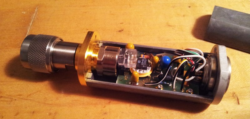
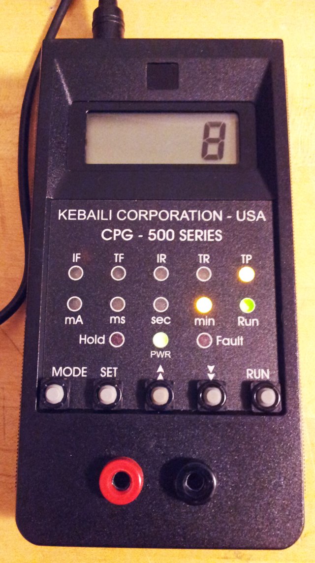
A rather rare guest in the workshop, a specialized power supply, for reverse pulse plating. Most of these are huge boxes used in the plating industry, with current rated in 10s of Amps, but this device is made for the semiconductor field, for depositing metal on silicon, for MEMS (micro-electro-mechanical) devices, etc. It’s a rather lightweight device, in a handheld case, powered by an external DC power supply.

cpg-500 kebaili

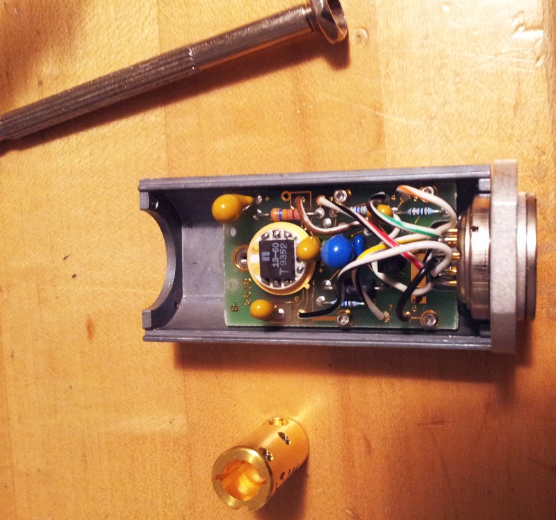
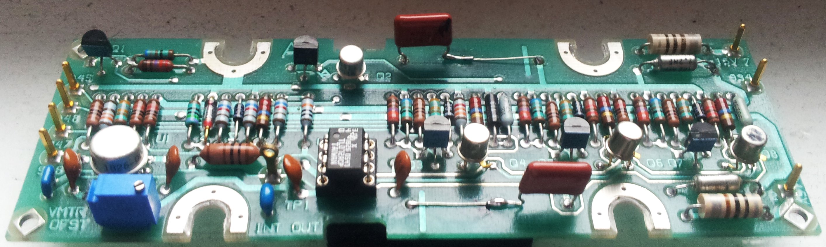
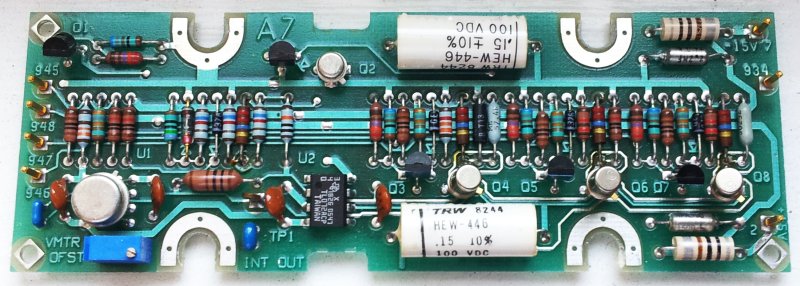
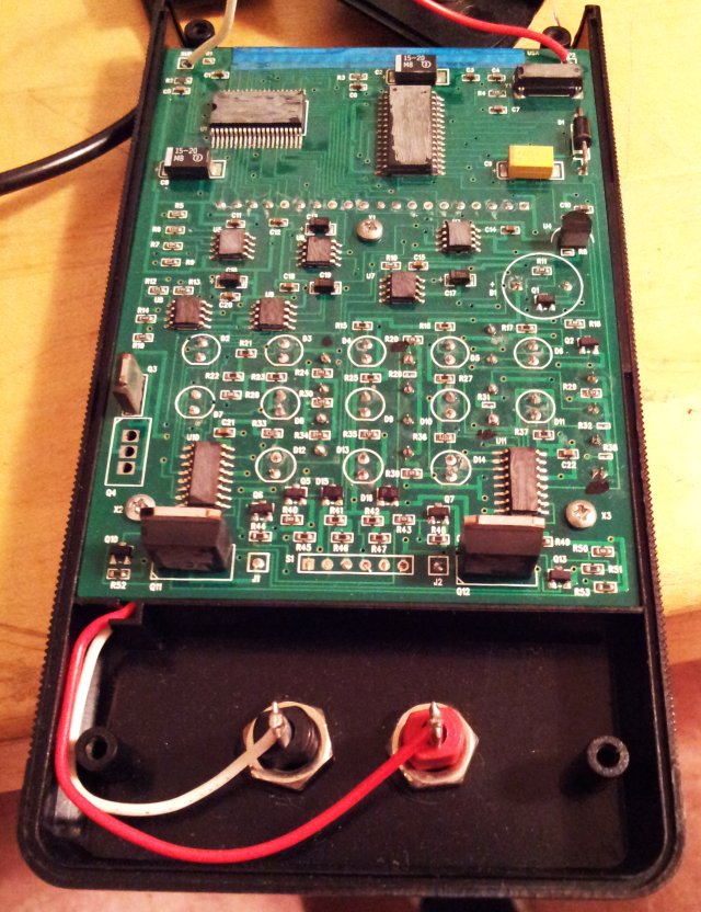
The internals show a construction which is more like a prototype than a fully engineered device. Epoxy glue is used to hold in the buttons, and Capton tape at various places. Well, some prototypes last forever, and it is certainly build to a good standard. The folks building it were very concerned about their design it seems, and removed all the marking from the parts used! Keep in mind, this is just a pulse current supply – why all the effort, and why make it so difficult to repair! Even more striking is the fact that the company manufacturing these is now out of business, with no information available whatsover, and no service provided (at least, I was able to obtain the user manual from the owner of the device). Please, leave the markings on the circuits, they are there for good reason – to let others fix the devices, when your greed and protective nature has ruined your business.

cpg-500 board

A few words about reverse pulse plating. You all know the through-hole plated circuits boards, plated vias, etc. These are made by electrochemically depositing copper, a method which Faraday and others invented long ago, but only in recent decades refinements were made to the current profiles to get nicely through-plated (and also filled) holes. Being able to deposit copper in cavities of any shape, etched into other materials, opens up a tremendous number of applications (e.g., complicated patters can be etched into silicon using the well-established methods of the semiconductor industry, then filled with copped – after removal of the silicon by selective etching, the small copper parts remain, resembling all the detail etched into the silicon).

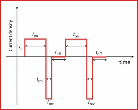
Here, the general pulse sequence: forward current pulse, reverse current pulse, idle time (no current).

cpg-500 reverse current plating generic

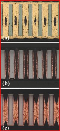
A plating example (not from my lab), (a) shows a not properly plated through-hole (cavity in center) resulting from conventional plating; (b) and (c) are pulse plated – one can see how nicely the copper is growing, even in the center. Needless to say, all can be adjusted by selecting the right mix of chemicals, and by optimizing the current levels and pulse duration for the desired results (filled hole, filled cavity, wall-plated hole, and so on). Typically pulse times are milliseconds. But can be 10s or 100s of milliseconds, in cases.

cpg-500 plating example generic

The CPG-500 has 3 current ranges, quite a flexible device, to cover applications from micrometers to square centimeters…. resolution is about 1:4000, about 12 effective bit.

cpg-500 current ranges

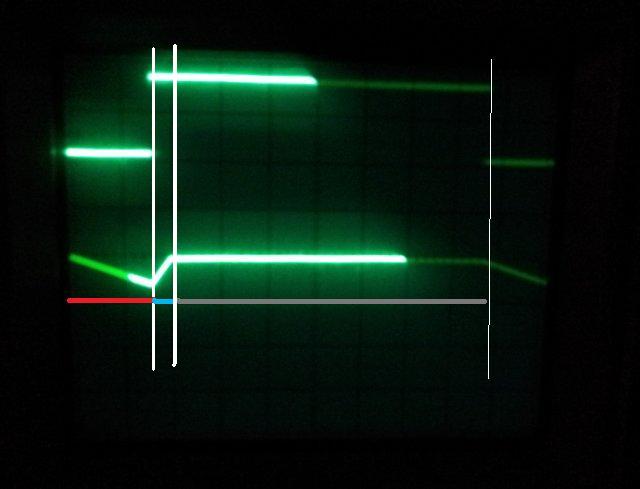
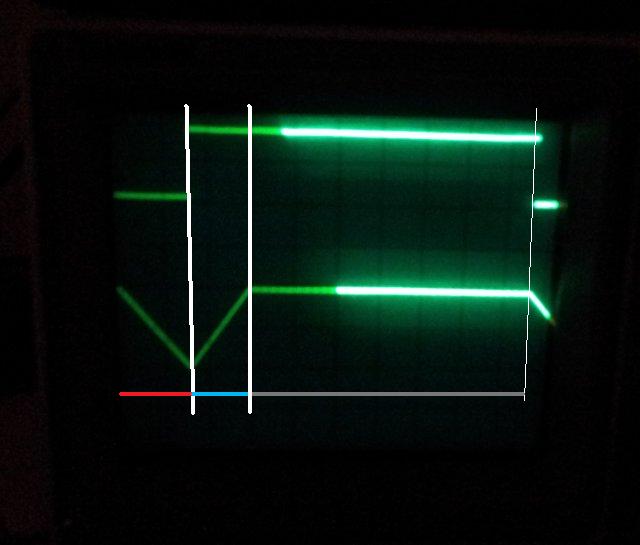
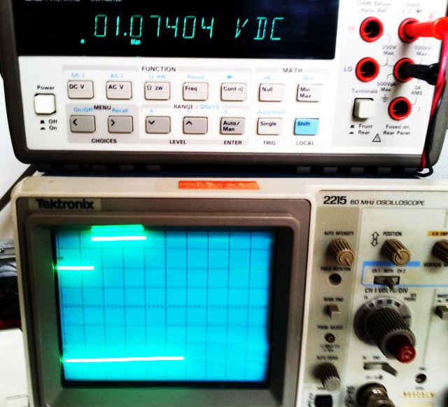
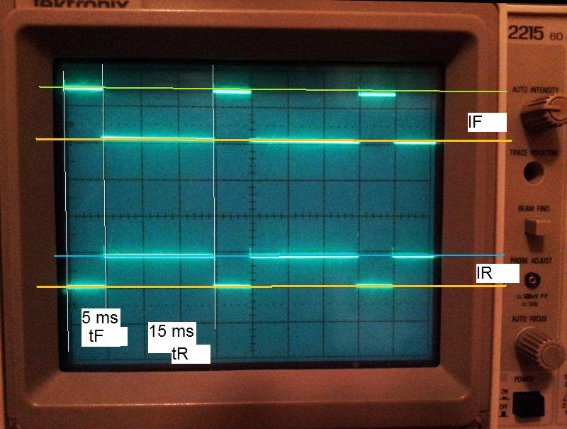
After some repair, no spectacular enought to write about, these are the output signals. Pretty clear how it works – lower trace is forward current, upper trace reverse current – during operation, the current sources is switched from one output to the other and back, grounding one of the outputs at a time. When switched off/when plating is finished, both outputs are switched off/high impedance, with no current flowing. Orange lines are 0 V ground potential of the power supply.

cpg-500 current test

Because of the way this bipolar operation is realized (by unipolar switching of current), probing the current requires a few tricks. A 100 Ohms resistor inserted in the current path (in series with an amp meter), and two oscilloscope probes.

cpg-500 current probing

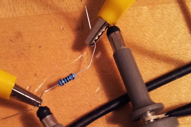
The scope is then used in ‘add inverse’ mode to subtract the two signals, resulting in the display of the actual forward and reverse currents, as one trace.

cpg-500 plating current example

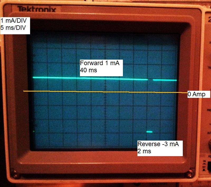
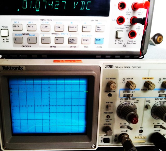
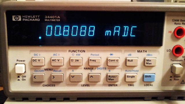
This is a quite typical waveform, the reverse current is 1.5-3x the forward current, at about 2-10% of the duty cycle. This example as 1 mA forward current, 3 mA reverse current, 40 ms forward, 2 ms reverse pulse (i.e., current ratio is 3, and time ratio is 20). This results in an average current of (40*1-2*3)/42=0.8095 mA. An, not really surprisingly, this is what the amp meter shows.

cpg-500 average current

Call it fixed!

HP 8481A Power Sensor: why are they all blown?

A remarkable HP product, the HP8481A sensor. It appeared on the market about 1974, and still today, these devices are very much thought after. It works from about 10 MHz to 18 GHz, -30 to +20 dBm.

Quite some detail about this sensor can be found in the HP Journal, 1974-09 edition (pages 19ff).
There is says that the sensor can withstand 300 mW power, and even 0.5 Watts for seveal days. Still, there are many sensors around that are blown – why do so many people connect them to 0.5+ W transmitters and destroy them along the way? I have no idea!

Here, a quick glance at the internals:

8481a view

8481a thermocouple chip

8481a thermocouple cross section

8481a schematic hp

8481a schematic

8481a exploded view

8481a power sensor

8481a shield

8481a open

8481a internal

8481a ferrites

8481a connector

8481a sensing element

Note the capacity values – measures: 3.5 nF at the input, 3.0 nF at the output. This is all real gold on sapphire substrate!

8481a capacitor values

HP 8970A Noise Figure Meter: A7 voltmeter assy fix

Finally, some capacitors arrived, Panasonic ECW FD type, polypropylene dielectric. These are very much suitable for any type of active filter or sample/hold circuits, thanks to their good capacitance stability, and low dielectric absorption.

8970a a7 assy cap replacement ecw-fd2w154jq

8970a ecwfd capacitor data

Dielectric adsorption, not something specified on the datasheet. So I did a quick test, using a 50 Volt power supply, a 100 Ohms resistor, and a high-impendance (10 GOhm or more) voltmeter. Test follows this sequence:
(1) Charge capacitor for about 10 minutes; make sure to limit charge current to a few 10s of mA.
(2) Discharge for 10 seconds, using a 100 Ohm resistor.
(3) Measure voltage and record maximum value (V_measured) – typically, this takes several seconds.
(4) Calculate: V_measured/50 Volt *100%, the number obtained is a measure of dielectric absorption, in %.

Results: 0.005% for the ECW FD (Panasonic brand, PP dielectric), and 0.09% for the original cap, HEW-446 series (TRW brand, PET dielectric). Not bad, rule of thumb says that PP has 5x lower absorption than PET, well, but don’t quote me on the numbers measured – these are just rough estimates, fair enough. Needless to say, the new capacitors will outperform the original ones by far – and hopefully last as long, or longer, 30+ years….

Another detail. Note the line on the top side of the A7 board, close to one terminal of the capacitor? This is the outer winding of the capacitive layer. This goes to ground. The ECW FD aren’t marked for their winding direction (these are non-polar caps, but still, there is an outer layer of foil, and an inner layer, and the outer layer does pick up more noise, and thus needs to go to the lower impedance connection). But the winding direction can easily be determined, just connect the capacitor to an oscilloscope probe, and hold the part between your fingers – then, swap the probe (switch ground and hot connection). You will see different levels of noise on the screen, mainly, 50/60 Hz hum. Select the connections for lowest noise, and the ground lead of the oscilloscope probe will then indicate the outer layer of the winding. Best, mark it with a felt pen.

8970a a7 assy caps replaced

USB RTL SDR 28.8 MHz Reference: dividers, PLL, success

With the 28.8 MHz VCO design established, all we need to move this project on are divers for the 28.8 MHz (VCO) and 10 MHz (Reference) signals, a slow-acting PLL, and some auxilliary circuitry to feed the 28.8 MHz back to the RTL SDR.

The 28.8 MHz and 10 MHz signals are AC coupled with about 1 kHz input impedance, this is quite common for any 10 MHz reference signal input (used for various kinds of test equipment). These signals are then amplified/limited by unbuffered inverters, 74HCU04. This is a very cost-effective and easy solution, the HCU04 has push-pull outputs, and input clamping diodes. Still, some clamp diodes have been added for the 10 MHz input, just in case.

28.8 mhz divider chain schematic

Looking at 28800 kHz, and 10000 kHz, 400 kHz is the largest common denominator. Accordingly, we need :72, and :25 division factors.

Division of the 10 MHz down to 400 kHz is accomplished by two 74LS90, but you can use other TTL decade dividers, these were just the circuits I had in stock.
28.8 to 400, a bit more tricky, first, divided by 8, using a 74LS293, and another LS293 that has two diodes, acting as an “OR”, to reset the counter when count 9 is reached.

Both 400 kHz signals are then compared use a flip-flop phase comparator, conveniently packaged in a 4046 PLL. For convenience, and to avoid digital noise on the 12 V rail powering the VCO, the 4046 is powered only from 5 V. This somehow limits the tuning output range, from close to 0 V, to about 3.1 V.

The loop filter is very slow acting, tens of seconds, because the objective of this PLL is to correct long-term drift of the 28.8 MHz reference, introduced by temperature, Xtal drift, etc., but otherwise not to impact its noise and oscillation characteristics.

28.8 mhz pll and loop filter schematic

The VCO (see earlier post, VCO design) uses a fixed capacitor to set the tuning offset, this was changed to 4.4 pF, and finally to 2.2 pF, to properly center the tuning voltage (V_tune, output of the PLL loop filter buffer) within the 4046 output range, at roughly 1.7 V.
Extentensive testing was carried out the ensure that the VCO starts up properly, even if extreme V_tune voltages are applied; as the 28.8 MHz Xtals used in the USB RTL SDR devices may vary, you will need to check the required tuning range and pullability of the Xtal. Some Xtals oscillators will stop oscillating, if you pull to frequency up or down too much, which might happen during PLL start-up. This can lead to an undesirable lock-up condition.

Here are the tuning characteristics, for 2p2, and 4p4 pF VCO capacitor values.

28.8 mhz tuning

This is the divider and PLL board. Sure it would be much nicer to have everything completely separated, in shielded cans, etc., but I did not go to such effort. Later testing will reveal if it has any bad consequences for the 28.8 MHz phase noise, but so far, I don’t see much noise – will do a more in-depth comparison later.

28.8 mhz pll boad

HP 8970A Noise Figure Meter: defective A7 voltmeter assembly – temporary fix

A broken noise figure meter, not really a good situation with so many tasks related to noise figures at hand, not only the noise source projects. So, another look at the A7 assembly. With the suspect TL072 opamp replaced by a less suitable, but known-working subsititute, the fault still comes and goes – well, maybe, in the end, the TL072 is not even at fault? There aren’t so many components around, so I checked for all the likely and unlikely things, and found – a defective integrating capacitor!

See the schematic – there are two of the same kind – C4 is the bad one (integrator cap; upper orange frame), C3 (auto-zero; lower orange frame) is fine.
8970a a7 assy schematic c3 c4 capacitors

0.15 µF, 100 V, Mylar, 1982 vintage, and after all these years, somehow, it has developed an intermittent fault (the first Mylar cap with such fault I have ever seen).

trw hew-446 0.15uF 100vdc

With no spare at hand in my tiny New Jersey workshop, I decided to swap the caps, using C3 as C4, and temporary mounted a 0.1 µF film capacitor (Wima FKM) as C3. For the auto-zero function, the exact value and leakage of the capacitor won’t matter so much, anyway.

a7 assy swapped cap

See, how nicely it works: red – integrator charged from input voltage; blue – integrator discharged by reference voltage; grey – auto-zero; this sequence repeats over and and over again, and the duration of the reference segment is determined, after applying the input voltage for a fixed time (all controlled by LS TTL logic on another board).

0.25 V input, 1.2 V reference.
a7 voltmeter 0.25 v input

1.0 V input, 1.2 V reference.
a7 voltmeter 1 v input

Some quick thoughts about the capacitor; typically, Mylar/PET/polyester caps aren’t the best for integrators, because of higher leakage current, and dielectric absorption, compared to, say, polypropylene caps. Maybe, at the time, HP engineers determined that the TL072 leakage current, and other leakage currents on the board would be much larger than any capacitor leakage current; or, they didn’t want to introduce specialized parts – these axial Mylar capacitors of TRW brand were quite common in 1970- early 1990 era HP gear. These are actually not metallized Mylar/PET, but film-foil capacitors (using discrete plastic and metal foil, similar to Wima FKS-3).

Look inside the dead cap – there actually are the plastic and metal foils.
mylar and metal film

For the next few weeks, this configuration will be sufficient; then I will check capacitor stock back at the main workshop; most likely there are some Wima/Epcos/TDK FPK or MKP (PP dielectric foil-foil or metallized PP foil) capacitors around; if not, then I will just fit a pair of good Mylar caps.

HP 8970A Noise Figure Meter: voltmeter assy (A7) defect

Not so good news today, after characterizing all kinds of noise sources, the 8970A stopped working. Can’t get it to calibrate properly, or to show any reasonable noise power values. A quick check revealed that the detector output (voltage proportional to the noise power measured) is good. But no proper display when activating the 8970A-internal volt meter (special functions 80, 81).

Checking various traces and signals – the issue seems to reside with the A7 assembly, voltmeter.
8907a a7 assy

Red – input voltage section; green – reference voltage section (about 1.2 V); blue – auto-zero section.
8970a a7 assy schematic

How it works, quite well-established dual-slope integration with autozero – a capacitor, initially at zero volts, is charged first from the input voltage, then from a (negative) reference voltage, until zero is reached again. The time it takes to do this directly relates to the input voltage.

See here, working example (sorry a bit dim- see the triangular shape in the lower left hand corner of the scope screen).
working trace

Here, non-working condition – integrator not working.
non-working trace

After checking various FETs, and timing signals – the TL072 integrator opamp appears to be the faulty device. It is a strange, intermittent fault – not triggered by vibration, but appears to be intermittent with no direct external cause – maybe a defective output stage of the opamp? Removed it from the circuit; unfortunately, all spare back at the main workshop in Germany, but fair enough will get some TL072s in soon.

tl072 defective

…. once repair is done, noise source project will continue asap!

TWS-N15 Noise Source: checking out some design alternatives

So far, we have mainly been discussing series type noise sources, i.e., noise sources where neither anode nor cathode are connected to ground. Another common design is shown here – the shunt configuration (one port of the noise generation element grounded).

noise source bfr93a shunt

The assembly, more or less just a little blob of solder with a few tiny parts inside… mostly, 0603 SMD format. The output attenuator (not shown) is a 14.5 dB(!), 18 GHz coaxial attenuator.

noise source bfr93a shunt assy

Some quick measurements, at bias currents of 2.5, 5 and 7 mA…. still, there seems to be a lot of 1/f noise (increase of noise power at lower frequencies). This is model #1, with a 22 nF capacitor (see schematic)

noise bfr93a shunt configuration 1

Don’t really see any advantage over the series variant of the noise source. But will test further.

…Progress on another front, ordered a set of PCBs – they can be used for various noise source configurations. Not yet a “prototype”, but need to see what kind of GHz performance is available from such design, and how reproducible it is. No current source yet on this PCB – will add later, or on a separate board – to limit shielding to the RF section.

noise source pcb 150827-2

TWS-N15 Noise Source: some RF transistors as noise generating devices

After testing some Zener diodes and regular transistors (see earlier posts), some attempts with high frequency transistors, to generate white noise (noise power constant with frequency).

So far we have found that Zener diodes generate high noise power, and are rather flat out to 1.5+ GHz (if proper package and mounting is chosen). However, there is appreciable 1/f noise (increase of noise power) below 100 MHz, and this is difficult the equilize with just plain R-C networks.

Another attempt, with regular tansistors – they don’t have enough noise power at high frequencies, past a few 100 MHz.

Now, finally, I have received some 6 GHz BFR93A and 22 GHz BFG410W transistors, from my stock of parts back home in Germany, and have put these to the test. Same circuit is used like before, with positive current fed into the emitter, and the base grounded via some resistors (transistor is run in emitter-base breakdown condition to generate noise).

These are the parts concerned, some general notes – the BRF93A is a very useful part for all kinds of RF applications, and available at low cost.

noise bfr93a

The BFG410W, it is also quite remarkable and I use it a lot for LNA (low-noise amplifier) designs – hard to beat at their cost, delivering considerable gain, at low power. Unbelievable what the semiconductor folks have been able to achieve, a 22 GHz transistor, for a few cents each!

noise bfg410w

Here, the ENR results, vs. bias current, in mA.

BFR93A
noise enr vs bias bfr93a
-note that the ENR increases at low bias current!

BFG410W
noise enr vs bias bfg410w

As can be seen, and don’t ask me why, the BFG410W generates much less noise. Some quick change of the attenuator pad – 4 dB less attenuation. Just to check if this has any effect (besides increasing output power) – all seems well behaved and power is increased without changing any of the general characteristics.

BFG410W – lower 3 traces are 390 ohms parallel, upper 3 traces are 130 ohms parallel output attentuator (390 ohm 0603 pad resistor, paralleled with 390 or 130 ohm 0603 resistor)
noise enr vs bias bfg410w 130 ohm pad

The BFG410W appears to have the best white noise characteristics so far, note that the measurements are still not too accurate, mainly for screening of parts. With proper bias current selection, flatness, 100 to 1000 MHz, <0.2 dB should be possible. Will do some more experimentation, and fine-tuning of the filter/equilization components; ideally, the noise power should be a bit higher, to be able to use a larger, well-matched attenuator, giving good output SWR. Also, I think it is now about time to fabricate some better HF boards (still using FR4, but precision made), to get a reproducible assembly, and to have several TWS-15N prototypes made and characterized.

TMS 2532 EPROM adapter: one byte every 50 ms…..

EPROM progammers seem like a thing of the past, still, they are very popular for test equipment repair, arcade games, and all kinds of other occasions where small amounts of data need to be stored in a bulky, fancy package.
Such programmers, mostly copies of the “Willem” design, are widely available, Made in China, and generally, these work pretty well. Well, as luck would have it, most of the ancient pieces of equipment use 2532 EPROMs, and just this kind is not supported by the common programmers, which support the 2732….. same capacity, different pin layout.

2732 pinout

tms2532-45

tms2532jl-45

To adapt the 2532/2532A (these only differ by their programming voltage, 25 V vs. 21 V – make sure the set it correctly) to the common 2732 programmers, the only thing you need is a small adapter, with a most complicated schematic (the only pins that change are 18, 20 and 21). Most of these EPROMs require programming pulse widths of about 50 ms, but often program OK with just 10 ms, or less.

2532 eprom adapter for programming schematic

2532 programming adapter view 2

2532 programming adapter view 1

TWS-N15 Noise Source: noise generating elements

Some trials with various low-cost noise generating circuit elements:

(1) Zener diodes
(2) Transistors B-E junctions in break-down mode
(3) Noise diodes – these are not being considered, not low cost.

For (1), a BZV55-12 diode was used, directly soldered on the traces of the noise source circuit described earlier.
For (2), as a first try, a BC238B transistor was used (with legs cut to very short length). Sure, I will try some RF transistors, but these are all back in the main workshop in Germany and will come over in a couple of weeks.

noise bc238b lin

noise bc238b log

The output, measured with a HP 8970A noise figure meter and some GPIB software to do this efficiently, it shows quite interesting behavior.

For the Zener diode, there is appreciable 1/f (pink) noise at <30 MHz, but the output is pretty much flat at higher frequencies. The transistor, well, it is working fine at lower frequencies, at 10 mA bias, the noise is flat-white up to about 300 MHz. But not enough noise at higher frequencies - maybe just not the right part for this purpose. These are just a few of the components tested, stay tuned.